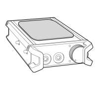
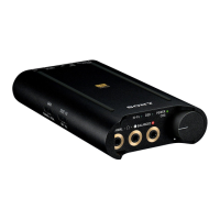
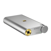
PHA-1A/1AEU
PHA-1A/1AEU
1010
For Schematic Diagrams.
Note:
• All capacitors are in μF unless otherwise noted. (p: pF) 50
WV or less are not indicated except for electrolytics and
tantalums.
• All resistors are in Ω and 1/4 W or less unless otherwise
specifi ed.
• C : Panel designation.
THIS NOTE IS COMMON FOR PRINTED WIRING BOARDS AND SCHEMATIC DIAGRAMS.
(In addition to this, the necessary note is printed in each block.)
• A : B+ Line.
• B : B– Line.
• Voltages and waveforms are dc with respect to ground
under no-signal conditions.
no mark
: POWER ON
• Voltages are taken with VOM (Input impedance 10 M).
Voltage variations may be noted due to normal production
tolerances.
• Waveforms are taken with a oscilloscope.
Voltage variations may be noted due to normal production
tolerances.
• Circled numbers refer to waveforms.
• Signal path.
F : AUDIO (ANALOG)
J : AUDIO (DIGITAL)
E : iPhone/iPad/iPod
j : WALKMAN/Xperia
• The voltage and waveform of CSP (chip size package)
cannot be measured, because its lead layout is different
from that of conventional IC.
For Printed Wiring Boards.
Note:
• X : Parts extracted from the component side.
• Y : Parts extracted from the conductor side.
• : Pattern from the side which enables seeing.
(The other layers’ patterns are not indicated.)
• Waveforms
– MAIN Board –
Caution:
Pattern face side:
(Conductor Side)
Parts face side:
(Component Side)
Parts on the pattern face side seen
from the pattern face are indicated.
Parts on the parts face side seen from
the parts face are indicated.
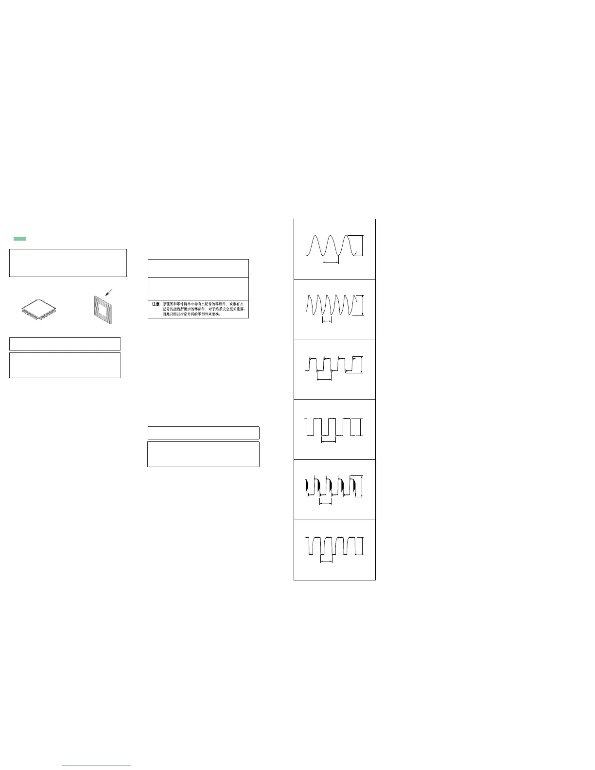
• Lead layouts
surface
CSP (Chip Size Package) Lead layout of conventional IC
* Replacement of IC704 on the MAIN board used in this unit
requires a special tool.
* Replacement of IC704 on the MAIN board used in this unit
requires a special tool.
Note: When replacing the MAIN board, be sure to re-
place the case simultaneously. Among the repair
parts, the MAIN board and case are supplied as
one unit.
Note: When replacing the MAIN board, be sure to re-
place the case simultaneously. Among the repair
parts, the MAIN board and case are supplied as
one unit.
5
IC500 6,7 (SW)
2 V/DIV, 500 ns/DIV
750 ns
8 Vp-p
6
IC501 9 (EXT)
1 V/DIV, 2 Ps/DIV
3.1 Ps
4.1 Vp-p
2
IC401 qk (MCLK_OUT)
1 V/DIV, 50 ns/DIV
59.5 ns
4.5 Vp-p
3
IC401 wj (BCLK_OUT)
1 V/DIV, 200 ns/DIV
470 ns
4 Vp-p
1
IC401 7 (CF2)
500 mV/DIV, 50 ns/DIV
83 ns
3 Vp-p
22.4 Ps
3.5 Vp-p
4
IC401 wk (LRCK_OUT)
1 V/DIV, 20 Ps/DIV
Note: The components identifi ed by mark 0 or
dotted line with mark 0 are critical for safety.
Replace only with part number specifi ed.
Note: Les composants identifi és par une marque
0 sont critiques pour la sécurité.
Ne les remplacer que par une piéce portant
le numéro spécifi é.