UFOELK - 2/21/2018 5:23 PM
HT-RT3
29
• IC Block Diagrams
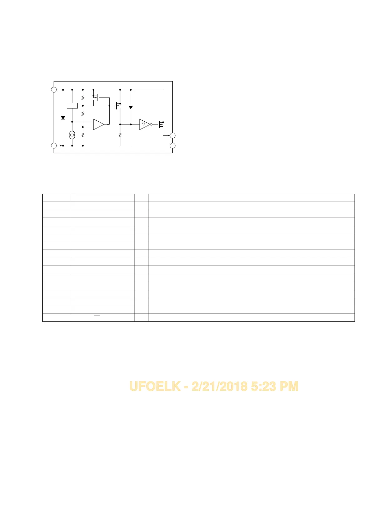
IC4002 PST8429UL (TOUCH BOARD)
GND 1
VDD
2
+
–
VREF
OUT4
CD
3
Ver. 1.1
• IC Pin Function Descriptions
TOUCH BOARD IC4001 CY8CMBR3108-LQXIT (TOUCH KEY CONTROLLER)
Pin No. Pin Name I/O Description
1, 2 CS0/PS0, CS1/PS1 - Fixed at “L” in this unit
3 CMOD - External capacitor connection terminal
4 VCC O Internal regulator output terminal
5 VDDIO - Power supply terminal (+3.3V)
6 VDD - Power supply terminal (+3.3V)
7 VSS - Ground terminal
8 CS4/GPO0 I/O Touch key input/output terminal Not used
9 CS5/GPO1 I VOL + touch key input terminal
10 CS6/GPO2 I VOL – touch key input terminal
11 CS7/GPO3/SH I PAIRING touch key input terminal
12 CS2/GUARD I
INPUT touch key input terminal
13 CS3 I Power touch key input terminal
14 I2C_SDA I/O Two-way I2C serial data bus with system controller
15 I2C_SCL I/O Two-way I2C serial data transfer clock signal bus with system controller
16 HI/BUZ O Interrupt signal output to the system controller