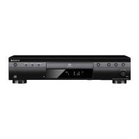
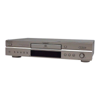
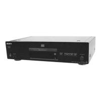
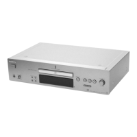
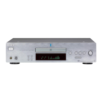
SCD-XE800
2
1. SERVICING NOTES ............................................. 3
2. DISASSEMBLY
2-1. Disassembly Flow ........................................................... 5
2-2. Case, Fuse (F001) ........................................................... 5
2-3. POWER Board ................................................................ 6
2-4. Panel (Loading) ............................................................... 6
2-5. Front Panel Block ........................................................... 7
2-6. CD Mechanism Deck Block
(CDM66F1-DVBU101) .................................................. 7
2-7. MAIN Board ................................................................... 8
2-8. Belt (LD), MOTOR Board,
Motor (L) Assy (Loading) (M001) ................................. 8
2-9. Base Unit ......................................................................... 9
2-10. Optical Pick-up Block (KHM-313CAB) ........................ 9
3. TEST MODE ............................................................ 10
4. DIAGRAMS
4-1. Block Diagram - RF/SERVO, MAIN Section - .............. 14
4-2. Block Diagram
- PANEL, POWER SUPPLY Section - ........................... 15
4-3. Schematic Diagram - MAIN Section (1/5) - ................... 17
4-4. Schematic Diagram - MAIN Section (2/5) - ................... 18
4-5. Schematic Diagram - MAIN Section (3/5) - ................... 19
4-6. Schematic Diagram - MAIN Section (4/5) - ................... 20
4-7. Schematic Diagram - MAIN Section (5/5) - ................... 21
4-8. Printed Wiring Board - MAIN Section (1/2) - ................ 22
4-9. Printed Wiring Boards - MAIN Section (2/2) - .............. 23
4-10. Printed Wiring Boards - PANEL Section - ..................... 24
4-11. Schematic Diagram - PANEL Section - .......................... 25
4-12. Printed Wiring Boards - POWER Section - .................... 26
4-13. Schematic Diagram - POWER Section - ........................ 27
5. EXPLODED VIEWS
5-1. Case, Front Panel Section ............................................... 36
5-2. Chassis Section ............................................................... 37
5-3. Mechanism Deck Section (CDM66F1-DVBU101) ........ 38
5-4. Base Unit Section ............................................................ 39
6. ELECTRICAL PARTS LIST .............................. 40
Accessories are given in the last of the electrical parts list.
TABLE OF CONTENTS
NOTES ON CHIP COMPONENT REPLACEMENT
• Never reuse a disconnected chip component.
• Notice that the minus side of a tantalum capacitor may be dam-
aged by heat.
FLEXIBLE CIRCUIT BOARD REPAIRING
• Keep the temperature of soldering iron around 270 °C during
repairing.
• Do not touch the soldering iron on the same conductor of the
circuit board (within 3 times).
• Be careful not to apply force on the conductor when soldering
or unsoldering.
SAFETY-RELATED COMPONENT WARNING!
COMPONENTS IDENTIFIED BY MARK 0 OR DOTTED LINE
WITH MARK 0 ON THE SCHEMATIC DIAGRAMS AND IN
THE PARTS LIST ARE CRITICAL TO SAFE OPERATION.
REPLACE THESE COMPONENTS WITH SONY PARTS
WHOSE PART NUMBERS APPEAR AS SHOWN IN THIS
MANUAL OR IN SUPPLEMENTS PUBLISHED BY SONY.
This appliance is classifi ed as
a CLASS 1 LASER product.
This marking is located on the
rear exterior.
CAUTION
Use of controls or adjustments or performance of procedures
other than those specifi ed herein may result in hazardous radia-
tion exposure.