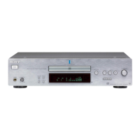
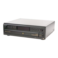
SCD-XE800
31
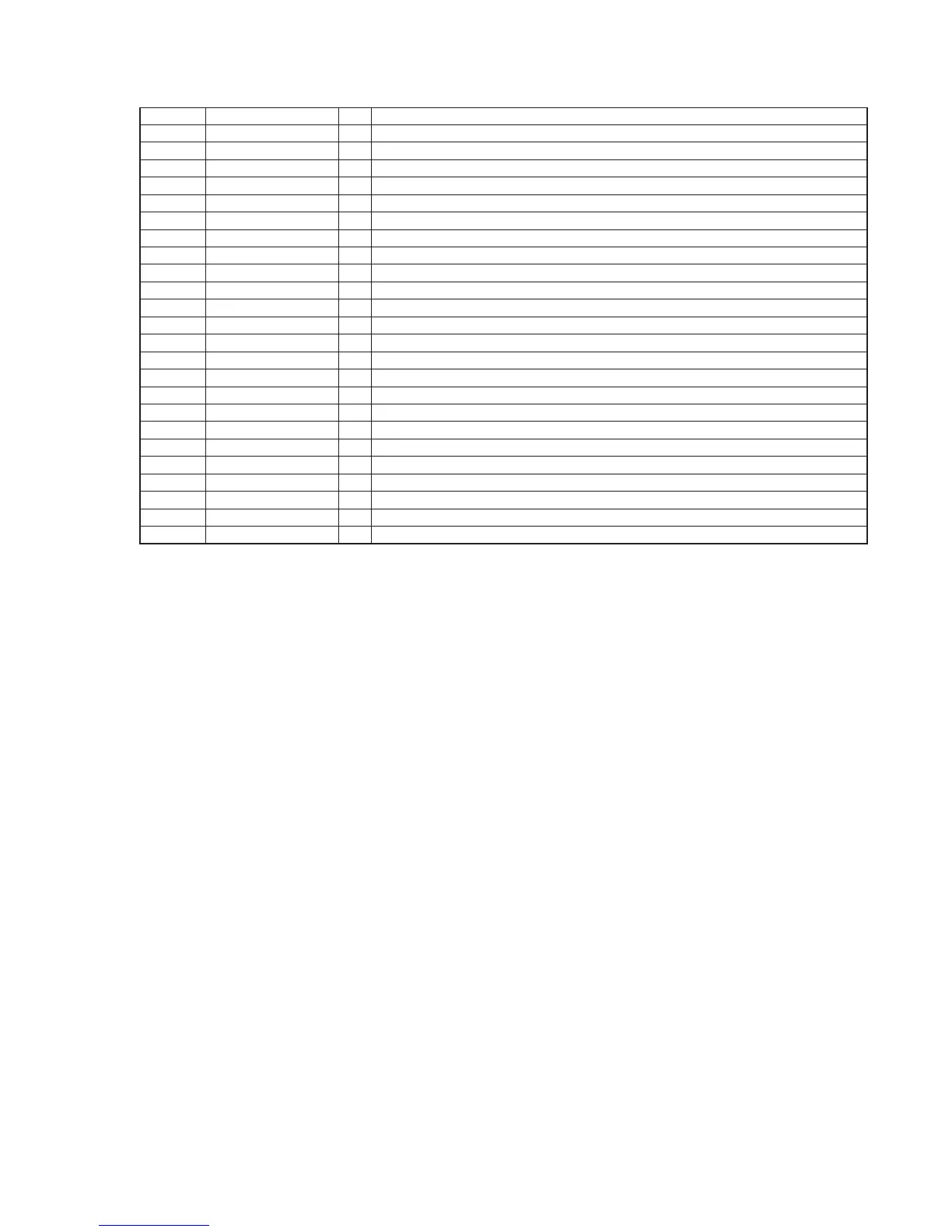
Pin No. Pin Name I/O Description
65 to 73 No Use O Not used
74 KEY_INT I Wake up signal input terminal
75 LED_LAT O Serial data latch pulse signal output terminal Not used
76 No Use O Not used
77 No Use I I2C Two-way data bus with the clock generator Fixed at “H” in this set
78 No Use I I2C data transfer clock signal input/output with the clock generator Fixed at “H” in this set
79 to 82 No Use O Not used
83 CKSW I Chucking detection switch input terminal
84 OCSW I Disc tray open/close detection switch input terminal “L”: disc tray is closed
85 No Use O Not used
86 No Use O Not used
87 No Use O Not used
88 DAC_CS1 O Chip select signal output to the D/A converter
89 LED_PLAY O Play LED drive signal output terminal “H”: LED on
90 LED_PAUSE O Pause LED drive signal output terminal “H”: LED on
91 No Use O Fixed at “L” in this set
92 DESTINATION I Setting terminal for the destination
93 MODEL I Setting terminal for the model
94, 95 KEY2, KEY1 I Front panel key input terminal
96 AVss - Ground terminal
97 KEY0 I Front panel key input terminal
98 Vref I Reference voltage (+3.3V) input terminal
99 AVcc - Power supply terminal (+3.3V)
100 No Use O Not used
 Loading...