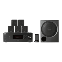
STR-KM5/KM7
57
Pin No. Pin Name I/O Description
52 MD1 - Operation mode specifi cation input pin
53 MD0 - Operation mode specifi cation input pin
54 RST - Reset input pin
55 HDMI_TX_INT I HDMI: Tx Interrupt port from HDMI-Tx Device
56 HDMI_SDA IO HDMI: Communication Line I2C SDA
57 HDMI_SCL O I2C Clk
58 HDMI_RX_INT I RX Interrupt
59 SI I Serial data input terminal (use for Firmware Flash Program)
60 SO O Serial data output terminal (use for Firmware Flash Program)
61 FLASH_CLK O Inline Programing Clock
62 UART_SEL O UART Selector
63 DSP_SPICS O Chip select signal output to DSP
64 DSP_SFLASH_HOLD O Hold signal output to the serial fl ash
65 DVCC - PA port power supply pin
66 DVSS - PA port power supply pin (GND)
67 DSP_RST O System reset signal output to the DSP “L” reset
68 DSP_INT I Interrupt status signal input from DSP
69 DSP_SEL_MULTI O Digital audio interface receiver / HDMI receiver signal selection signal output terminal
70 DSP_NPCM I SPDIF / IIS NPCM signal input from digital audio interface receiver / HDMI receiver
71 DSP_ERROR I SPDIF / IIS Error signal input from digital audio interface receiver / HDMI receiver
72 DIR_INT I Interrupt signal input from DIR
73 POWER_RY O Power relay control signal output
74 DIR_SIGNAL I Audio serial data input from the digital audio interface receiver
75 DIR_RST O Reset signal output to the digital audio interface receiver
76 DIR_CE O Latch signal output for DIR IC
77 NO USE - Not Used
78 DIR_MISO I Serial data input from DIR
79 DIR_XSTATE I Clock selection signal input from the digital audio interface receiver
80 STOP I AC off detection signal input
81 FAN_BLK I Fan Fail Detect
82 FUSE_DET I Fuse open detect signal input
83 V_COMP_SW2 O Component video selection signal output to the video amplifi er
84 V_MUTE O Video mute signal output for COMPONENT VIDEO SELECT IC
85 V_SEL_SW1 O Composite video selection signal output to the video amplifi er
86 V_SEL_SW2 O Composite video selection signal output to the video amplifi er
87 HDMI_NON_LPCM O HDMI: Non LPCM Stream Info Line Notifi cation
88 COM_CLK O Data clock signal output for DIR IC and 8 CH DAC IC
89 COM_DATA O Data output for DIR IC and 8 CH DAC IC
90 VCC - Power supply pin
91 VSS - Power supply pin (GND)
92 X1 - Main oscillator connecting pin
93 X0 - Main oscillator connecting pin
94 DAC_LATCH O Latch signal output for DAC
95 DAC_MUTE O Mute signal output for 8CH DAC IC
96 DIR FSRATE I L/R sampling clock signal input from the digital audio interface receiver and HDMI receiver
97 EVOL_CLK O Serial data transfer clock signal output to the electrical volume
98 EVOL_DATA O Serial data output to electrical volume
99 E2P_SDA IO Two-way data bus with the EEPROM
100 E2P_SCLK O Serial data transfer clock signal output to the EEPROM
Ver. 1.1