PVM-1353MD/1453MD
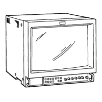
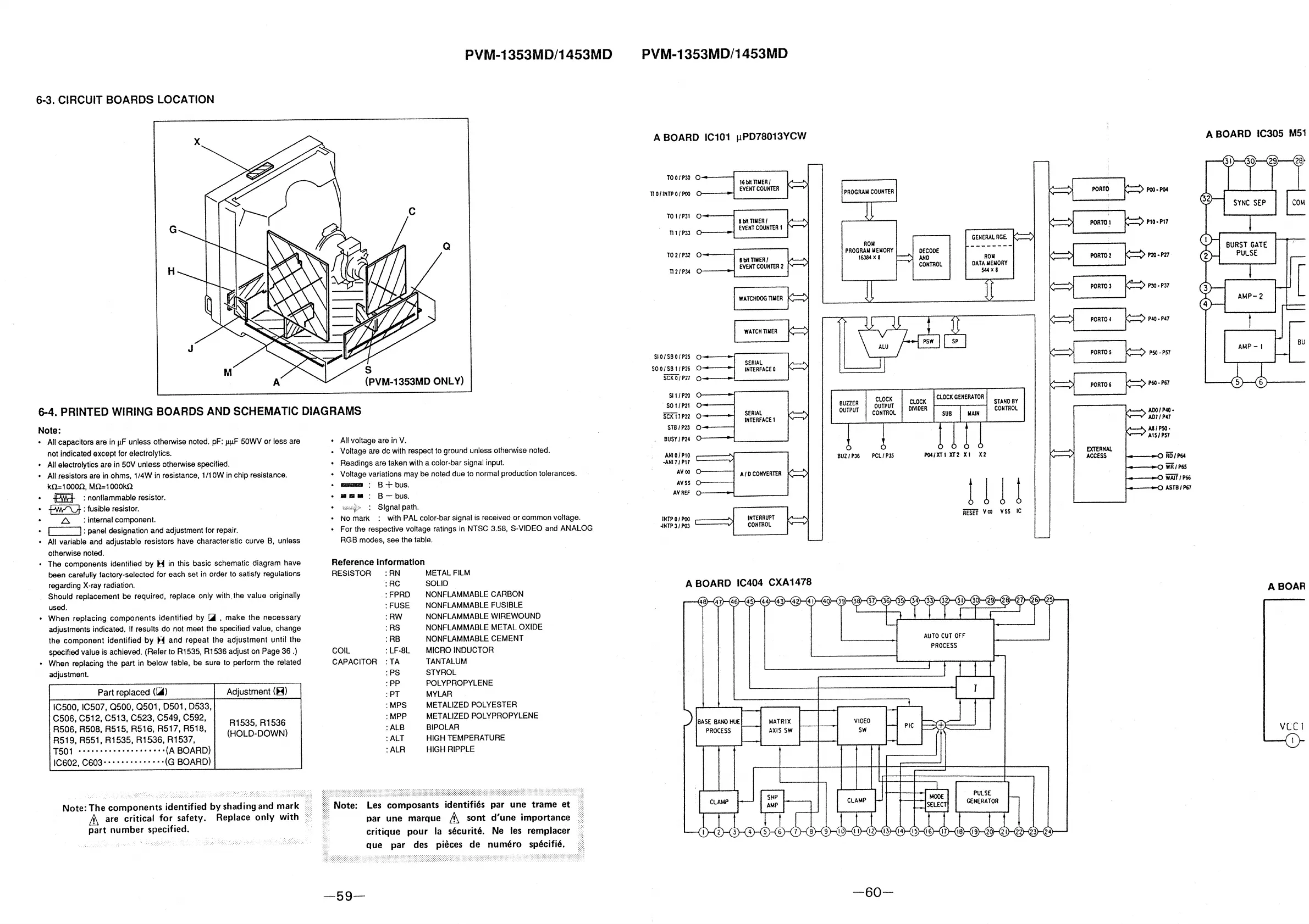
6-3. CIRCUIT BOARDS LOCATION
X
G
Q
H
M
s
(PVM-1353MD ONLY)
6-4. PRINTED WIRING BOARDS AND SCHEMATIC DIAGRAMS
Note:
• All capacitors are in µF unless otherwise noted. pF: µµF 50WV or less are
not indicated except for electrolytics.
• All electrolytics are in 50V unless otherwise specified.
All resistors are in ohms, 1/4W in resistance, 1/10W in chip resistance.
k!l= 1 ooon. Mil= 1 0001<n
m. : nonflammable resistor.
•
~
: fusible resistor.
6 : internal component.
c=J : panel designation and adjustment for repair.
All variable and adjustable resistors have characteristic curve B, unless
otherwise noted.
The components identified by
R in this basic schematic diagram have
been carefully factory-selected for each set in order to satisfy regulations
regarding X-ray radiation.
Should replacement
be required, replace only with. the value originally
used.
When replacing components identified by
~
, make the necessary
adjustments indicated.
If results do not meet the specified value, change
the component Identified
by H and repeat the adjustment until the
specified value is achieved. (Refer to R1535, R1536 adjust on Page 36 .)
When replacing the part in below table,
be sure to perform the related
adjustment.
Part replaced (Gill)
Adjustment (8)
ICSOO, IC507, QSOO, 0501, D501, D533,
C506, C512, C513, C523, C549, C592,
R1535,R1536
R506, R508, R515, R516, R517, R518,
(HOLD-DOWN)
R519, R551, R1535, R1536, R1537,
T501 • • ·• • • • • • • • •
········(A BOARD)
IC602, C603 • • • • • • • • • • • • • ·(G BOARD)
Note: The components identified by shading and mark
Lt are critical for safety. Replace only with
part number specified.
All voltage are in V.
Voltage are de with respect to ground unless otherwise noted.
Readings are taken with a color-bar signal input.
• Voltage variations may be noted due to normal production tolerances.
- B+bus.
•••: B-bus.
Signal path.
No
man<. : with PAL color-bar signal is received or common voltage.
For the respective voltage ratings in NTSC 3.58, S-VIDEO and ANALOG
RGB modes, see the table.
Reference Information
RESISTOR : RN METAL FILM
: RC SOLID
: FPRD NONFLAMMABLE CARBON
:FUSE
NONFLAMMABLE FUSIBLE
:AW
NONFLAMMABLE WIREWOUND
:RS
NONFLAMMABLE METAL OXIDE
:RB
NONFLAMMABLE CEMENT
COIL
: LF-8l
MICRO INDUCTOR
CAPACITOR :TA
TANTALUM
-59-
:PS
STYROL
:PP
POLYPROPYLENE
:PT
MYLAR
:MPS
METALIZED POL VESTER
:MPP
METALIZED POLYPROPYLENE
:ALB
BIPOLAR
:ALT
HIGH TEMPERATURE
:ALR
HIGH RIPPLE
Les composants identifies par une trame et
par une marque
& sont d'une importance
critique pour
la securite. Ne les remplacer
aue par des
pieces de numero specifie.
PVM-1353MD/1453MD
A BOARD IC101 µPD78013VCW
A BOARD IC305 M51
TOO/PJO
0
16bN llllERI
110/INTPO/POO
Ml!T COUNTER
PROGRAM COUNTl;R
PORTO
POI). PO,!
T01/P31 0
111 /Pl3
Sb111lt1ER/
PORT01
P10, P17
EVEKT COUNTER 1
GENERAL RGE.
ROIi
--------
T02/Pl2 0
ll 2/P34
PROGRAM !IE!IORY
OECOOE
Sbl11l11EII/
16384 X 8
A/10
ROM
PORT02
P20-P27
EVEKT COUNTER 2
CONTROL
OATA MEMORY
S44 X 8
PORT03
PJO,PJ7
WATCHOOG
ll!IER
PORTO
I
PIQ, P47
WATCHllllER
AMP- I
SU
SIO/SBO/P2S 0
PORTOS
PSO • PS7
SERIAL
SOO/S81/P26
0
INTERFACE 0
SCK 0/ P27
0
PORT06
P60 · P6T
SI 1 /PZQ
sot /P21
SCK 171'12
CLOCK GENERA
TOR
CLOCK
CLOCK
STANO BY
BUZZER
OUTPUT
SERIAL
OUTPUT
CONTROL
DMOER
CONT!lOL
ADO/ P40 •
INTERFACE 1
A07 / P47
SIB I P23
o-
AJIPSO•
BUSY/ P24
A1S/PS7
Al!IOiP10
BUZI PJ6
Pct/ P35
P0,1/XT1
XT2 X1
EXTERNAL
X2
ACCESS R0/1'64
-AHi 7 I PH
AVOO
AVSS
AV
REF
A IO CONVERTER
wiitffi
1 l
l
1
WAirl~
ASTB/P61
1NTP
01 POO
film V oo
VSS IC
INTERRUPT
~NTP 3 I POJ
CONTROL
A BOARD IC404 CXA1478
A
BOAR
VCCl
-60-