2
3
4
5
AB C D E F G H
8-28-2
VPL-S900E, VPL-S900M, VPL-S900U
1
QA -A SIDE-
SUFFIX: -15
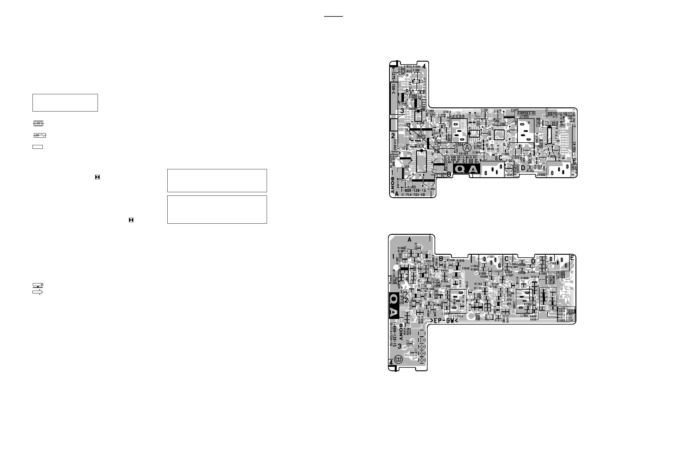
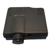
8-2. SCHEMATIC DIAGRAMS/PRINTED WIRING BOARDS
QA BOARD
QA -B SIDE-
SUFFIX: -15
QA
QA BOARD
*: B SIDE
*D1001 D-2
*D1002 C-1
*D1003 C-1
*D1004 D-1
D1005 D-1
D1007 B-2
*D1008 B-2
*D1009 D-2
*D1010 D-2
D1011 B-2
*D1012 B-2
D1013 B-2
D1014 A-3
D1015 A-3
D1016 A-2
IC1001 D-2
IC1006 A-2
IC1007 A-1
IC1008 C-2
IC1009 C-2
Q1001 D-2
*Q1002 D-2
*Q1003 B-2
Q1004 B-2
Q1005 D-2
Q1007 B-2
Q1008 D-2
*Q1011 A-1
*Q1012 A-2
Q1013 A-2
Q1014 A-2
Note:
• All capacitors are in µF unless otherwise noted. pF: µµF 50WV
or less are not indicated except for electrolytics.
• Indication of resistance, which does not have one for rating
electrical power, is as follows.
Pitch: 5 mm
Rating electrical power 1/4W
• All resistors are in ohms. (1M: 1000kΩ, 1k: 1000Ω)
• : nonflammable resistor.
• Chip resister are 1/10W unless otherwise noted.
• : fusible resistor.
• ¢ : internal component.
• : panel designation and adjustment repair.
• All variable and adjustable resistors have characteristic curve
B, unless otherwise noted.
• METAL CHIP (:RN, :RN-CP) resister in 1%, 0.5%, 1/4W un-
less otherwise specified.
• The components identified by
in this basic schematic dia-
gram have been carefully factory-selected for each set in or-
der to satisfy regulations regarding X-ray radiation.
Should replacement be required, replace only with the value
originally used.
• When replacing components identified by , make the nec-
essary adjustments indicated, If results do not meet the speci-
fied value change the component identified by and repeat
the adjustment until the specified value is achieved. (Refer to
page 4-1 and 4-2.)
• All voltages are in V.
• Reading are taken with Component color-bar signal (R.G.B
SYNC) input.
• Voltage are dc with respect to ground unless otherwise noted.
• no mark : 14G1/14G5 series and comon
( ) : 20G1 series
• Voltage variation may be noted due to normal production
tolerancd.
• : B+, B– line
•
: signal path
• Circled numbers are waveforms reference.
The components identified marked ! are
critical for safety.
Replace only with the part number specified.
Les composants identifiés par une marque
! sont critiques pour la sécurité.
Ne les remplacer que par une piéce portant
le numéro spécifié.
Reference information
RESISTOR : RN METAL FILM
: RC SOLID
: FPRD NONFLAMMABLE CARBON
: FUSE NONFLAMMABLE FUSIBLE
: RW NONFLAMMABLE WIREWOUND
: RS NONFLAMMABLE METAL OXIDE
: RB NONFLAMMABLE CEMENT
COIL : LF-8L MICRO INDUCTOR
CAPACITOR : TA TANTALUM
: PS STYROL
: PP POLYPROPYLENE
: PT MYLAR
: MPS METALIZED POLYESTER
: MPP METALIZED POLYPROPYLENE
: ALB BIPOLAR
: ALT HIGH TEMPERATURE
: ALR HIGH RIPPLE