99
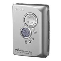
WM-FX488
Pin No. Pin name I/O Description
SECTION 4
DIAGRAMS
4-1. EXPLANATION OF IC TERMINALS
IC701 TC9329FA-CFX1740 (SYSTEM CONTROL)
1 to 4 COM 1 to 4 O LCD common drive
5 to 19 S 1 to 15 O LCD segment drive
20 S0 O Not used (OPEN)
21 to 22 K01 to 02 O Key output
23 to 26 K 1 to 4 I Key input
27 VDD – Power supply
28 BEEP O Beep signal output
29 FWD/REV CTL O FWD/REV head selection output
30 BAND1 O Tuner mode selection output
31 BAND2 O Tuner mode selection output
32 AMP CTL O Amplifier B+ switch ON/OFF control signal output
33 NC – Not used (OPEN)
34 BATT CHECK I Battery voltage check terminal
35 IF IN 1 I Tuner IF frequency input
36 HOLD SW I Hold switch input
37 GND – Ground
38 OSC IN I Tuner OSC frequency input
39 VDD – Power supply terminal
40 DO (OT) O Tunning data output
41 VREG – Capacitor connection terminal
42 IF REQ O IF request output for tuner
43 TAPE I Tape power switch input
44 RADIO ON O Tuner ON/OFF output
45 LOCAL/DX, O Tuner sensitivity/tape type selection output
STEREO/MONO
46 FWD/REV SW I FWD/REV switch input
47 P-CTL O Power switch ON/OFF output
48 MODEL1 I Distination select terminal
49 MODEL2 I Distination select terminal
50 PRE CTL O PRE mute output
51 MUTE CTL O PRE mute signal output
52 MB CTL O Megabass control signal output
53 AVLS CTL O AVSL control signal output
54 RESET I Reset signal input
55 X-OUT O System clock output (75kHz)
56 X-IN I System clock input (75kHz)
57 GND – Ground terminal
58 VDB – Capacitor conection terminal
59 C1 – Capacitor conection terminal
60 C2 – Capacitor conection terminal
61 VEE – Capacitor conection terminal
62 C3 – Capacitor conection terminal
63 C4 – Capacitor conection terminal
64 VLCD – Capacitor conection terminal
Note on Schematic Diagram
• All capacitors are in µF unless otherwise noted. pF: µµF 50 WV or
less are not indicated except for electrolytics and tantalums.
• All resistors are in Ω and
1
/
4
W or less unless otherwise specified.
•
f
: internal component.
• : B+ Line.
• H : adjustment for repair.
• Power voltage is dc 1.5V and fed with regulated dc power supply
from battery terminal.
•Voltages and waveforms are dc with respect to ground under no-
signal (detuned) conditions.
• no mark : FM (RADIO SECTION), PLAY (TAPE SECTION)
(): AM
•Voltages are taken with a VOM (Input impedance 10 MΩ).
Voltage variations may be noted due to normal production toler-
ances.
•Waveforms are taken with a oscilloscope.
Voltage variations may be noted due to normal production toler-
ances.
• Circled numbers refer to waveforms.
• Signal path.
F : FM
f : AM
E : PB
• Abbreviation
CH : Chinese
E: No indication of country of origin
6E : Indication of country of origin
Note on Printed Wiring Board
• X : parts extracted from the component side.
• a : Through hole.
• : Pattern from the side which enables seeing.
(The other layers' patterns are not indicated.)
Caution:
Pattern face side: Parts on the pattern face side seen from the
(Side B) pattern face are indicated.
Parts face side: Parts on the parts face side seen from the
(Side A) parts face are indicated.
• Abbreviation
CH : Chinese
E: No indication of country of origin
6E : Indication of country of origin
z
Waveforms
1
IC701 tg
VOLT/DIV : 1V AC
TIME/DIV : 5 µsec
X-OUT
2.9 Vp-
 Loading...