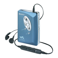
WM-EX527
1313
6-2. NOTE FOR PRINTED WIRING BOARD AND SCHEMATIC DIAGRAM
Note on Printed Wiring Board:
• X : parts extracted from the component side.
• Y : parts extracted from the conductor side.
•
z
: Through hole.
•
f
: internal component.
• : Pattern from the side which enables seeing.
(The other layers' patterns are not indicated.)
Caution:
Pattern face side: Parts on the pattern face side seen from
(Side B) the pattern face are indicated.
Parts face side: Parts on the parts face side seen from
(Side A) the parts face are indicated.
Note on Schematic Diagram:
• All capacitors are in µF unless otherwise noted. pF: µµF
50 WV or less are not indicated except for electrolytics
and tantalums.
• All resistors are in Ω and
1
/
4
W or less unless otherwise
specified.
•
f
: internal component.
• C : panel designation.
• A : B+ Line.
• H : adjustment for repair.
•Total current is measured with no cassette installed.
•Power voltage is dc 1.5 V and fed with regulated dc power
supply from battery terminal.
•Voltages and waveforms are dc with respect to ground in
playback mode.
no mark : PLAYBACK
•Voltages are taken with a VOM (Input impedance 10 MΩ).
Voltage variations may be noted due to normal produc-
tion tolerances.
•Waveforms are taken with a oscilloscope.
Voltage variations may be noted due to normal produc-
tion tolerances.
• Circled numbers refer to waveforms.
• Signal path.
E : PLAYBACK
3 Vp-p
10 µs
23.2 mVp-p
1.7 ms
2.1 Vp-p
250 ns
23.2 mVp-p
1.7 ms
•Waveforms
1 IC702 4 (LX)
2 IC701 5 (OSC IN)
3 IC701 wj (X1)
4 IC601 5 (OSC)
w
w
w
.
x
i
a
o
y
u
1
6
3
.
c
o
m
Q
Q
3
7
6
3
1
5
1
5
0
9
9
2
8
9
4
2
9
8
T
E
L
1
3
9
4
2
2
9
6
5
1
3
9
9
2
8
9
4
2
9
8
0
5
1
5
1
3
6
7
3
Q
Q
TEL 13942296513 QQ 376315150 892498299
TEL 13942296513 QQ 376315150 892498299
http://www.xiaoyu163.com
http://www.xiaoyu163.com
 Loading...