WM-FS220
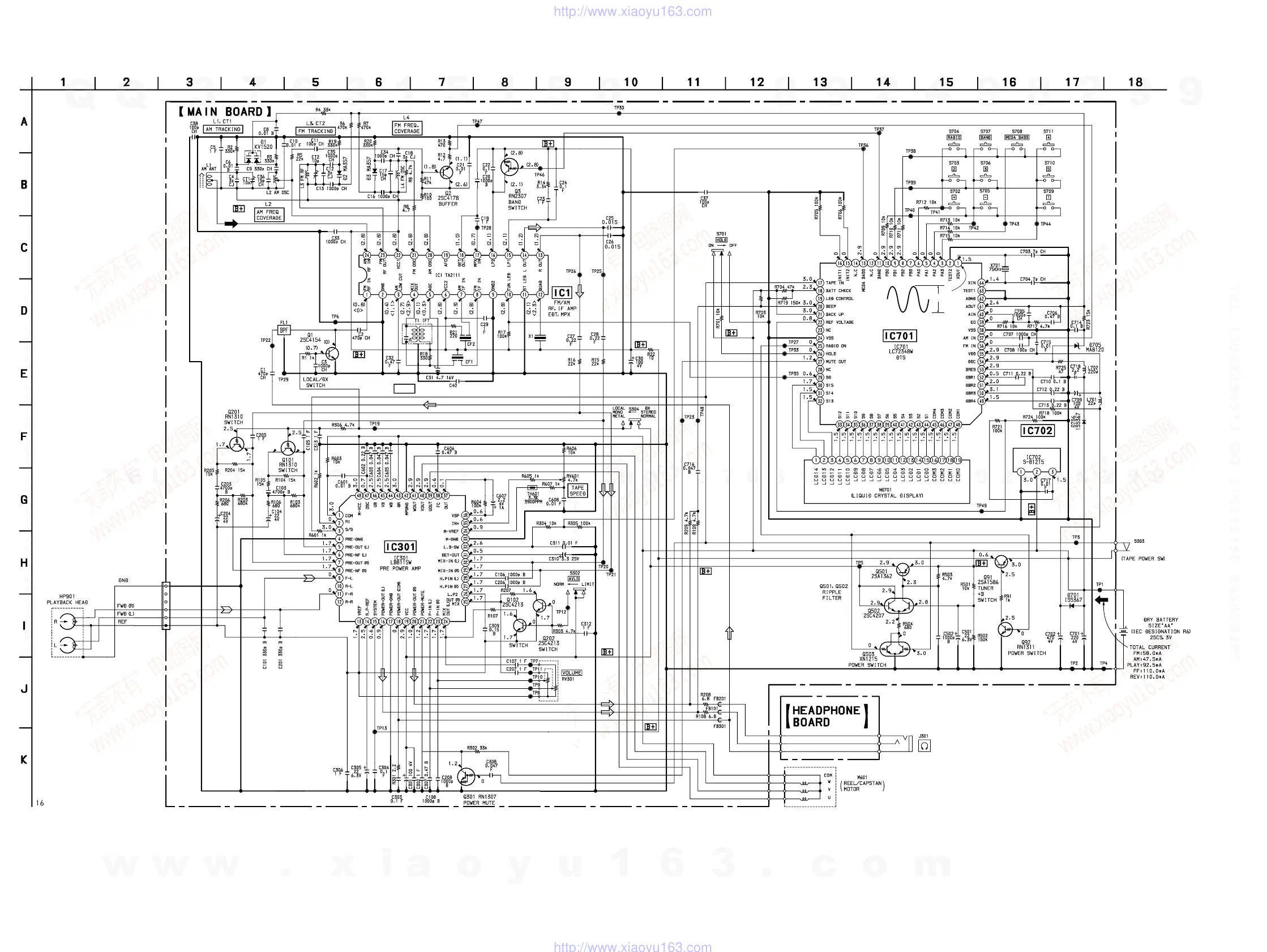
6-3. SCHEMATIC DIAGRAM
1.7
1.7
100P
150
150
2.1Vp-p
13.3µsec
500mV/div
5
µsec/div
+1.5V REG.
CN301
T1
AM IF
(2.8)
(2.8)
— 13 — — 14 —
Note on Schematic Diagram:
• All capacitors are in µF unless otherwise noted. pF: µµF
50 WV or less are not indicated except for electrolytics
and tantalums.
• All resistors are in Ω and
1
/
4
W or less unless otherwise
specified.
• C : panel designation.
• U : B+ Line.
• H : adjustment for repair.
• Power voltage is dc 3 V and fed with regulated dc power
supply from battery terminal.
• Voltages are dc with respect to ground under no-signal
(detuned) conditions.
no mark : PB
( ) : FM
< > : AM
• Voltages are taken with a VOM (Input impedance 10 MΩ).
Voltage variations may be noted due to normal produc-
tion tolerances.
• Signal path.
F : FM
f : AM
E : PB
• Refer to page 10 for IC Block Diagrams.
• Refer to page 17 for IC Pin Function.
w
w
w
.
x
i
a
o
y
u
1
6
3
.
c
o
m
Q
Q
3
7
6
3
1
5
1
5
0
9
9
2
8
9
4
2
9
8
T
E
L
1
3
9
4
2
2
9
6
5
1
3
9
9
2
8
9
4
2
9
8
0
5
1
5
1
3
6
7
3
Q
Q
TEL 13942296513 QQ 376315150 892498299
TEL 13942296513 QQ 376315150 892498299
http://www.xiaoyu163.com
http://www.xiaoyu163.com

 Loading...