8
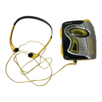
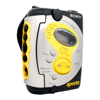
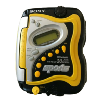
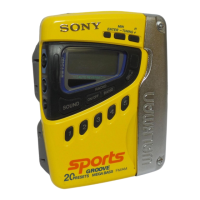
WM-FS555/FS556
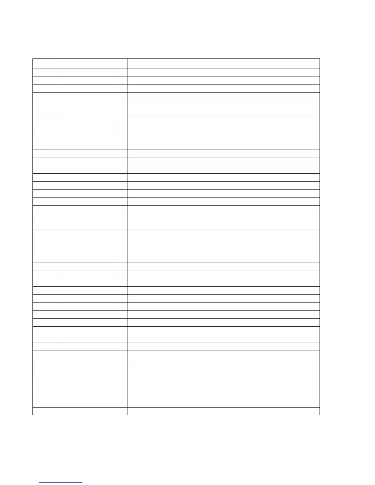
Pin No. Pin name I/O Description
SECTION 4
DIAGRAMS
4-1. EXPLANATION OF IC TERMINALS
IC701 TC9329FA-CFX1740 (SYSTEM CONTROL)
1 – 4 COMI-4 O LCD common drive.
5 – 19 S1-15 O LCD segment drive.
20 – 22 K01-03 O Key output.
23 – 26 K1-4 I Key input.
27 VDD – Power supply terminal.
28 BEEP O Beep signal output.
29 FWD/REV CTL O FWD/REV head selection output.
30 BAND1 O Band selection output.
31 BAND2 O Band selection output..
32 AMP CTL O Amplifier B+ switch ON/OFF control.
33 NC – Not used (OPEN).
34 BATT CHECK O Battery voltage check terminal.
35 IF IN 1 I IF input terminal.
36 HOLD SW I Hold switch input.
37 GND – Ground terminal.
38 OSC IN I OSC input from tuner.
39 VDD – Power supply terminal.
40 DO (OT) O Tuner B+ switch ON/OFF contorol.
41 VREG – Capacitor connection terminal.
42 IF REQ O IF request output for tuner.
43 TAPE I Tape power switch input.
44 RADIO ON O Tuner ON/OFF output.
45 LOCAL/DX, O Tuner sensitivity/tape type selection output.
NORM/MET
46 FWD/REV SW I FWD/REV switch input.
47 P-CTL O Power switch ON/OFF output
48 MODEL1 I Distination select terminal.
49 MODEL2 I Distination select terminal.
50 PRE CTL O PRE mute output.
51 MUTE CTL O PRE mute signal output.
52 MB CTL O Megabass control signal output.
53 AVLS CTL O AVSL control signal output.
54 RESET I Reset signal input.
55 X-OUT O System clock output (75kHz).
56 X-IN I System clock input (75kHz).
57 GND – Ground terminal.
58 VDB – Capacitor conection terminal.
59 C1 – Capacitor conection terminal.
60 C2 – Capacitor conection terminal.
61 VEE – Capacitor conection terminal.
62 C3 – Capacitor conection terminal.
63 C4 – Capacitor conection terminal.
64 VLCD – Capacitor conection terminal.
 Loading...