– 13 – – 15 –– 14 –
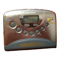
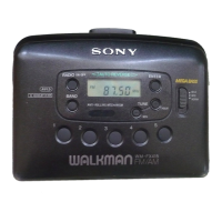
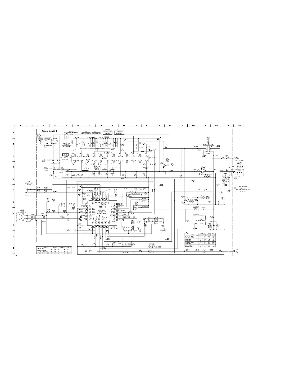
WM-FX193/FX195
4-3. SCHEMATIC DIAGRAM
Note:
• All capacitors are in µF unless otherwise noted. pF: µµF
50 WV or less are not indicated except for electrolytics
and tantalums.
• All resistors are in Ω and
1
/
4
W or less unless otherwise
specified.
•
f
: internal component.
• U : B+ Line.
• Power voltage is dc 3V and fed with regulated dc power
supply from external power voltage jack (J301).
no mark : FM
( ) : AM
< > : TAPE PLAY
• Voltages are taken with a VOM (Input impedance 10 MΩ).
Voltage variations may be noted due to normal produc-
tion tolerances.
• Signal path.
F : FM
E : PB
• Abbreviation
CND : Canadian
EA : Saudi Arabia
CH : Chinese
E : Indication of country of origin
E9 : No Indication of country of origin
CEV : Ukraine, Hungary, Czech
E5, E6 : South America
FR : French
 Loading...