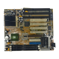
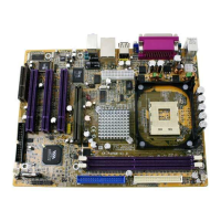
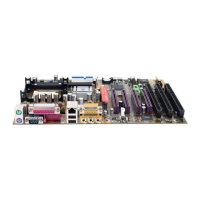
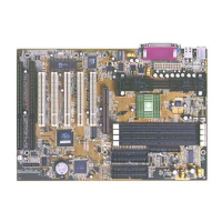
Hardware Setup
SY-7IZB+N
22
2-3.14
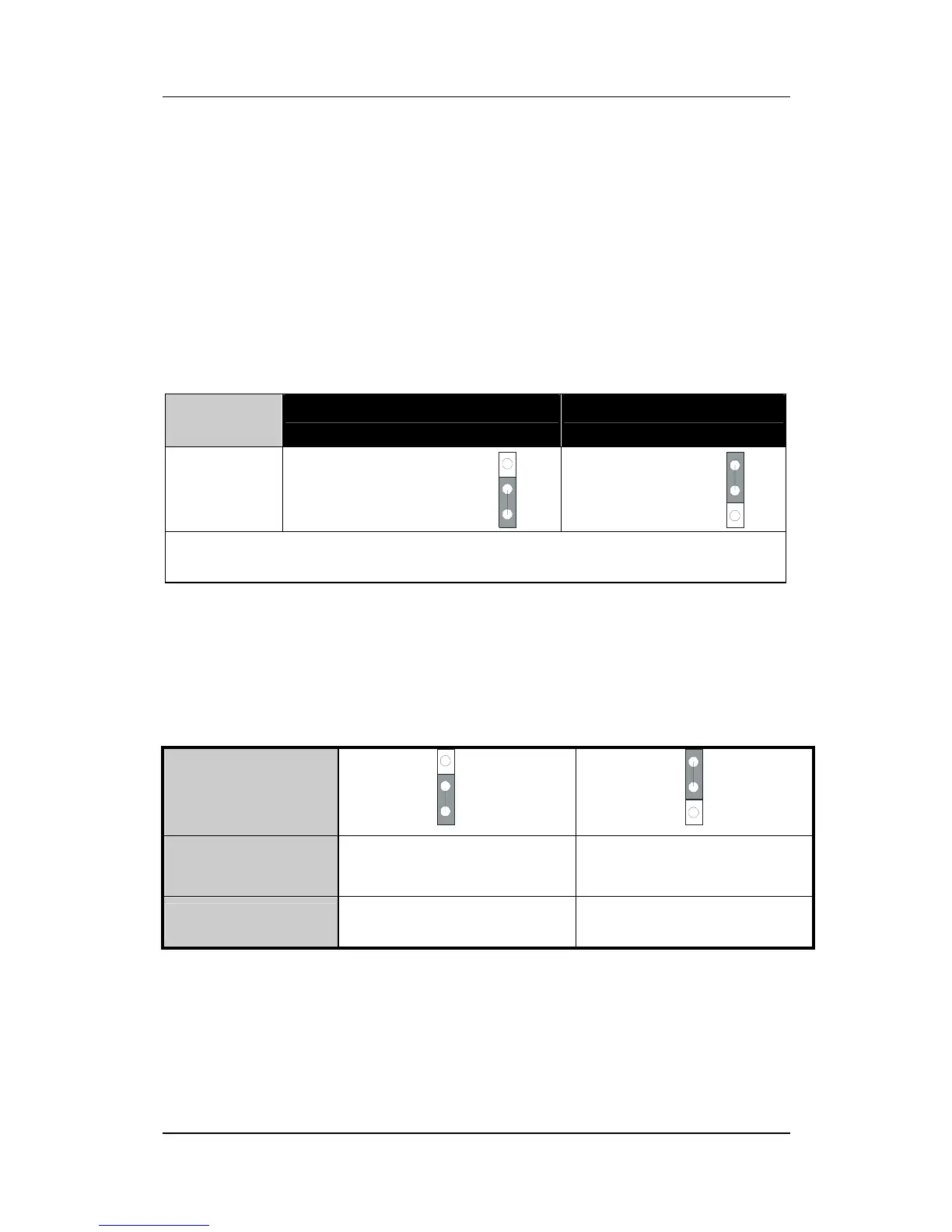
CMOS Clearing (JP5)
In some cases the CMOS memory may contain wrong data, follow
the steps below to clear CMOS memory.
1. Clear the CMOS memory by momentarily shorting pin 2-3 on
jumper JP5. This jumper can be easily identified by its white
colored cap.
2. Then put the jumper back to 1-2 to allow writing new of data
into the CMOS memory.
CMOS
Clearing
Clear CMOS Data Retain CMOS Data
JP5
Setting
Short pin 2-3 for
at least 5 seconds
to clear the CMOS
Short pin 1-2
to retain new
settings
Note: You must unplug the ATX power cable from the ATX power
connector when performing the CMOS Clear operation.
2-3.15
Set JP9 for power up FSB clock and AGP bus clock.
JP9 is used to adjust AGP bus clock frequency depending on the
value of the front side bus (FSB) clock, also the setting of the JP9
determines the power up FSB clock which will remain effective until
the BIOS set the FSB clock to the CMOS setting.
JP9 Setting
Power up FSB
Clock
66MHz 100MHz
AGP Clock
AGP Clock =
FSB Clock
÷
1
AGP Clock =
FSB Clock
÷
1.5
Note: The specification of maximum AGP bus Clock frequency
is 66.6MHz.
∗
Set JP9 to pin 1-2 short when you use a FSB 100MHz CPU.
∗
Set JP9 to pin 2-3 short when you use a FSB 66MHz CPU.
∗
Set JP9 to pin 1-2 short when you use a FSB 66MHz CPU but want
to over clock the FSB clock to 100MHz via the BIOS setting.
2
1
3
2
1
3
2
1
3
2
1
3
 Loading...