RF I/O stage
Note that PA0 is also connected to ARDUINO
®
and ST morpho connectors as GPIO, depending on the use case
that can generate conflict with B1. In this case, it possible to remove the connection of B1 (SB11 OFF).
Table 8. I/O configuration for the physical user interface
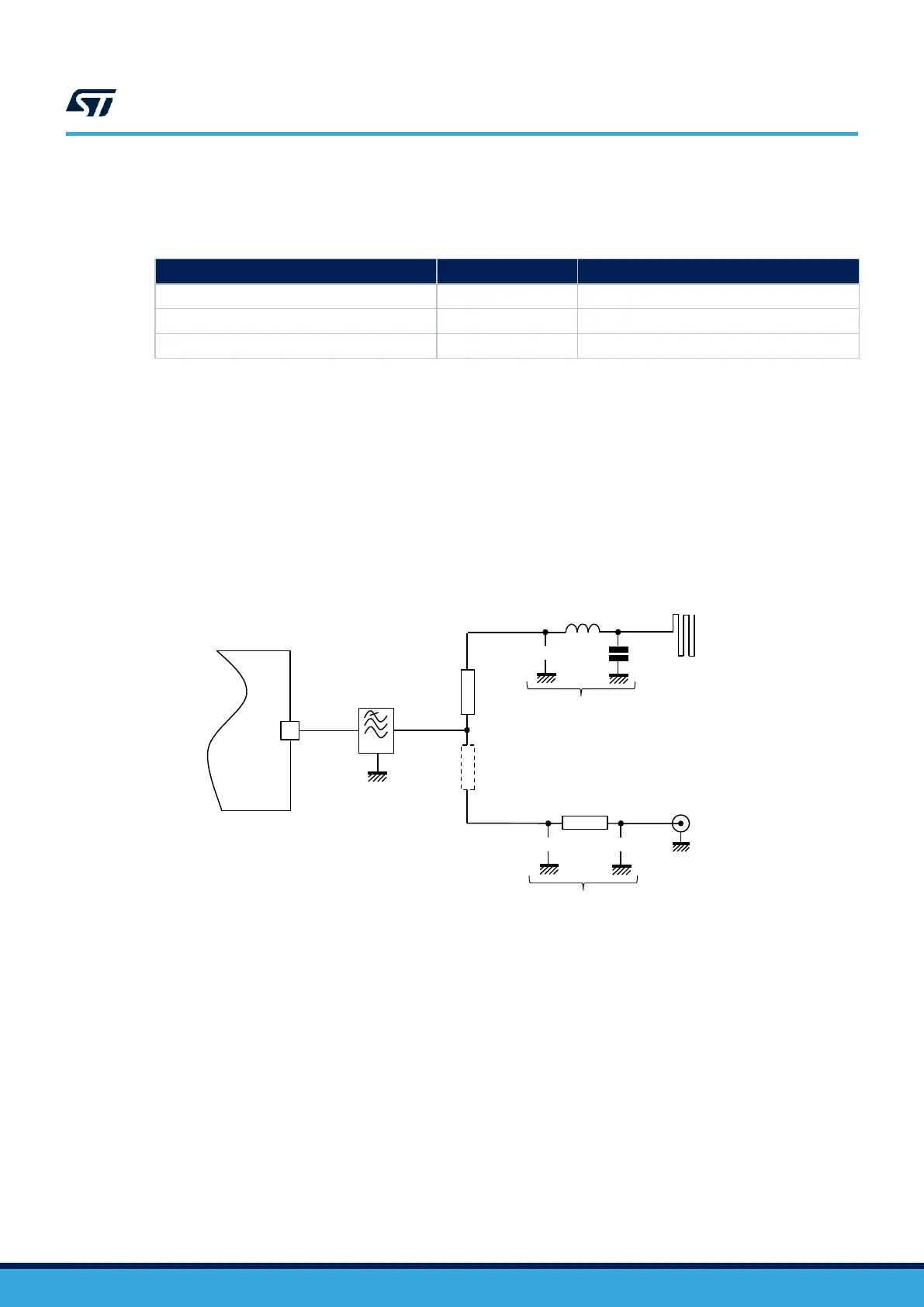
7.7 RF I/O stage
The RF output stage is configured by default to use a PCB antenna. Nevertheless, for laboratory characterization,
it is possible to use an SMA connector (not fitted by default).
Figure 14 shows the RF output stage schematic. On the I/O pin, a specific component manufactured by
STMicroelectronics allows to match the pin to 50 Ω and embeds a low pass filter which allows satisfying the
certification requirements.
Figure 14. RF I/O stage
ST Restricted
LPF
21
STM32WB55RG
SMA
R5
nc
0R
R13
C39 C40
MLPF-WB55-01E3
U13
3n6
L1
C36
PCB
Antenna
C37
nc
nc
nc
1p2
Optional network
if necessary to match
an external antenna
Matching network
of PCB antenna
R1
0R
J2
The components C36, L1, and C37 build the matching network of the PCB antenna. The footprint couple R1 and
R5 allows switching the direction of the RF I/O. If R1 is ON (default), the PCB antenna is used. If the 0 Ω resistor
presents on the R1 footprint is moved on the R5 footprint the SMA direction is used. C39, R13, and C40 are
available footprints to build a matching network for an external antenna. By default, the connection to SMA is
direct without matching network). R13 is 0 Ω resistor, C39 and C40 are OFF.

 Loading...