Hardware layout and configuration UM2407
32/50 UM2407 Rev 2
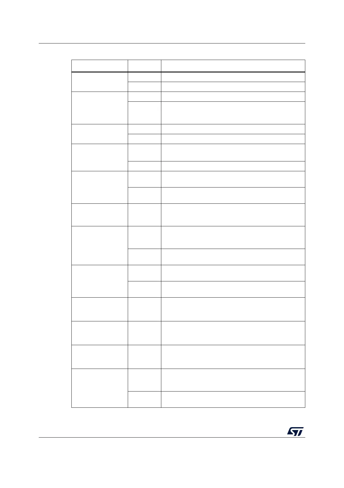
SB59 (PG6)
ON PG6 is connected to QSPI_CS (SB61 must be OFF).
OFF PG6 is used as GPIO on the ST morpho connector (CN12).
SB63 (PB2)
ON PB2 is connected to QSPI_CLK. (SB69 must be OFF)
OFF
PB2 is not connected to QSPI_CLK and can be used as
COMP1_INP (SB69 ON) or used as GPIO on the ST morpho
connector CN12. (SB69 OFF)
SB71, SB73
(PE6)
ON, OFF PE6 is connected to SAI_A_SD (D59 of CN9)
OFF, ON PE6 is connected to TIMER_A_BKIN2 (D38 of CN10)
SB67 (PE2)
ON
PE2 is connected to SAI_A_MCLK (D56 of CN9).
QSPI_BK1_IO2 cannot be used (D31 of CN10).
OFF PE2 is used as QSPI_BK1_IO2 (D31 of CN10).
SB53 (PC2) and
SB60 (PF10)
ON
ADC_IN are connected to A4 and A5 (pin 9 and 11) on the ST
Zio connector CN9. Thus SB55 and SB62 must be OFF
OFF
ADC_IN are connected to A4 and A5 (pin 9 and 11) on the ST
Zio connector CN9. Thus SB55 and SB62 can be ON (I
2
C)
SB65 (PF11) OFF
On NUCLEO-H723ZG, NUCLEO-H743ZI2, and NUCLEO-
H753ZI, PF11 is used only as GPIO on the ST morpho
connector (CN12) and must not be used as ADC_IN.
I
2
C
SB55 (PB9) and SB62
(PB8)
ON
PB9 and PB8 (I2C) are connected to A4 and A5 (pin 9 and
11) on the ST Zio connector CN9. Thus SB60 and SB53 must
be OFF
OFF
PB9 and PB8 (I2C) are not connected to A4 and A5 (pin 9
and 11) on the ST Zio connector CN9.
SB28 and SB70 (PE9)
ON, OFF
PE9 is used as TIMER_A_PWM1 (Pin 4) on the ST Zio
connector CN10.
OFF, ON
PE9 is used as COMP2_INP (Pin 15) on the ST Zio
connector CN9.
SB37 (PF12) and
SB38 (PF4)
OFF, ON
ADC_IN is connected to A6 (pin 7) on the ST Zio connector
CN10.
PF12 must not be used as ADC_IN (SB37 must be OFF)
SB48 (PF5) and SB49
(PF13)
ON, OFF
ADC_IN is connected to A7 (pin 9) on the ST Zio connector
CN10.
PF13 must not be used as ADC_IN (SB49 must be OFF)
SB50 (PF14) and
SB54 (PF6)
OFF, ON
ADC_IN is connected to A8 (pin 11) on the ST Zio connector
CN10.
PF14 must not be used as ADC_IN (SB50 must be OFF)
SB5
OFF
NUCLEO-H723ZG, NUCLEO-H743ZI2, and NUCLEO-
H753ZI support 1V8 and 3V3 for VDD_MCU. Thus U10 level
shifter is needed and SB5 must be OFF.
ON
If the MCU is supplied with 3V3, U10 can be by-passed and
SB5 can be ON.
1. The default SBx state is shown in bold.
Table 14. Solder bridge and jumper configuration (continued)
Bridge State
(1)
Description

 Loading...