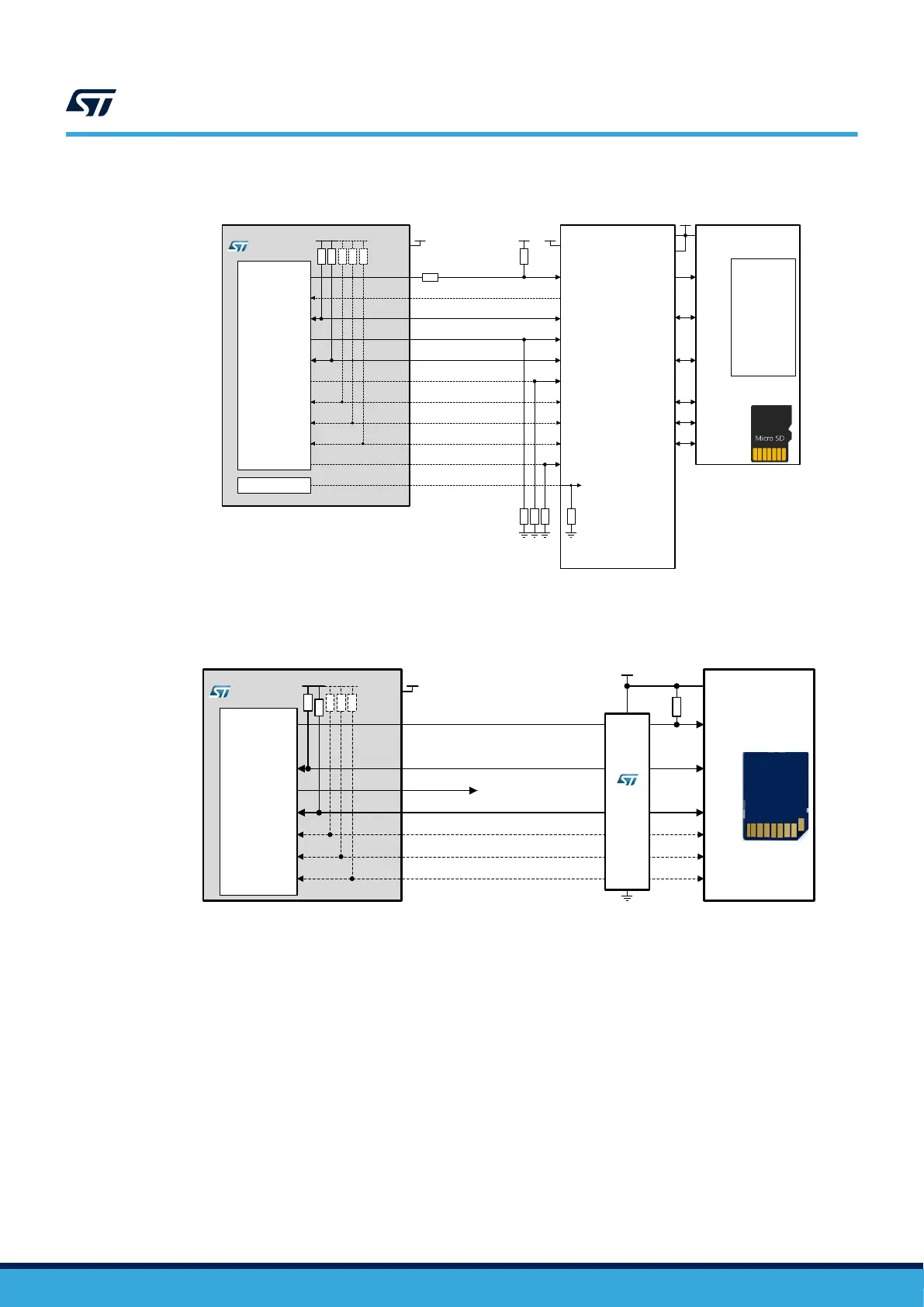
Figure 21. microSD card interconnection example
VDD
STM32H7
PC12
SDMMC1_CK
PD2
SDMMC1_CMD
PC8
SDMMC1_D0
PB9
SDMMC1_CDIR
PC6
SDMMC1_D0DIR
PB8
SDMMC1_CKIN
PC9
SDMMC1_D1
PC7
SDMMC1_D123DIR
PC10
SDMMC1_D2
PC11
SDMMC1_D3
VDD
R
PU
SDMMC1
R
PU
10k
VDD
10k
10k
10k
SD Card
Level Translator
(e.g. IP4856CX25)
GPIOx
Pxx
GPIOxx
0 = 3.3V Card signalling
1 = 1.8V Card signalling
VDD_ SD
SEL
V
CCA
V
SUPPLY
V
SD_REF
microSD Card
Socket
CMD
DAT0
DAT1
DAT2
DAT3
CLK
VDD
CLK_IN
CLK_FB
CMD_H
DIR_CMD
DATA0_H
DIR_0
DATA1_H
DATA2_H
DATA3_H
DIR_1_3
CLK_SD
CMD_SD
DATA0_SD
DATA1_SD
DATA2_SD
DATA3_SD
22
VDD
VDD
VDD is not
switched
between 1.8V
and 3.3V
Stays always
at 3.3V even
in fast mode
(only the
interfaces are
switched)
Figure 22. SD card interconnection example
STM32H7
PC12
SDMMC1_CK
PD2
SDMMC1_CMD
PC8
SDMMC1_D0
PB9
SDMMC1_CDIR
PC9
SDMMC1_D1
PC10
SDMMC1_D2
PC11
SDMMC1_D3
VDD
R
PU
SDMMC1
R
PU
VDD_SD
SD Card
Socket
CMD
DAT0
DAT1
DAT2
DAT3
CLK
VDD
Open (toggles during
SD-card boot)
Only default 3.3 V Card signaling
supported without level Translator
EMIF06-
USD05F3
VDD
VDD > 2.9 V
10k
9.4.2 Flexible memory controller (FMC) interface
Interface connectivity
The FMC controller and in particular SDRAM memory controller are composed of many signals, most of them
have a similar functionality and work together. The controller I/O signals could be split in four groups as follow:
• An address group which consists of row/column address and bank address.
• A command group which includes the row address strobe (NRAS), the column address strobe (NCAS), and
the write enable (SDWE).
• A control group which includes a chip select bank1 and bank2 (SDNE0/1), a clock enable bank1 and bank2
(SDCKE0/1), and an output byte mask for the write access (DQM).
AN5419
High speed signal layout
AN5419 - Rev 2
page 37/50
 Loading...


