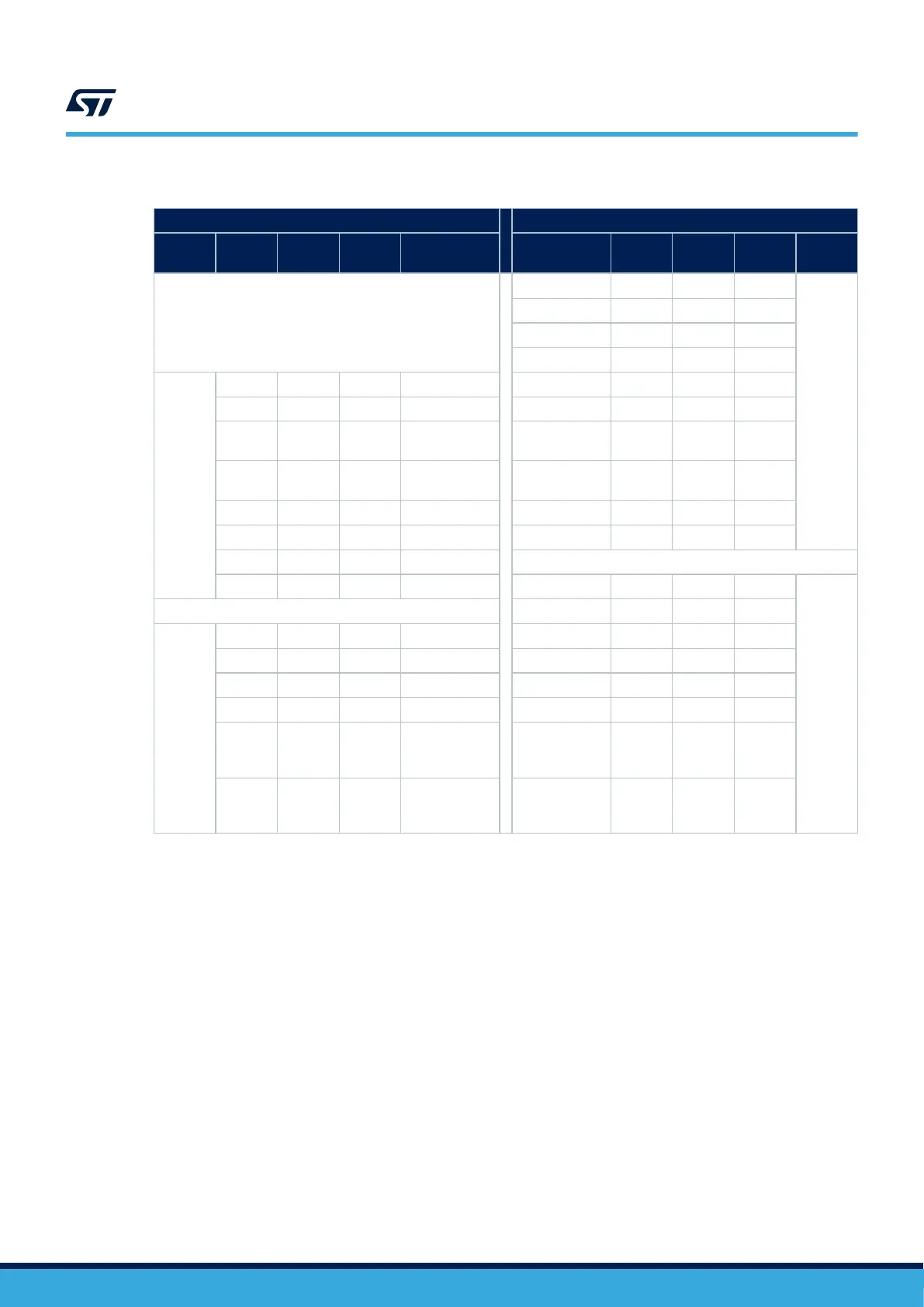
Table 23. ARDUINO
®
Uno V3 compatible connectors
Left connectors Right connectors
CN No. Pin No.
Pin
Name
MCU Pin Function Function MCU Pin
Pin
Name
Pin No. CN No.
-
-
I2C4_SCL PF14 D15 10
CN4
Digital
I2C4_SDA PF15 D14 9
AVDD - AVDD 8
Ground - GND 7
CN5
Power
1 - - 5V_IN test SPI5_SCK PF7 D13 6
2 IOREF - 3V3 Ref SPI5_MISO PF8 D12 5
3 NRST NRST Reset
TIM23_CH4,
SPI5_MOSI
PF9 D11 4
4 3V3 - 3V3 output
TIM23_CH1,
SPI5_NSS
PF6 D10 3
5 5V - 5V I/O TIM4_CH2 PB7 D9 2
6 GND - Ground - PE3 D8 1
7 GND - Ground -
8 VIN - Power input - PG5 D7 8
CN8
Digital
- TIM4_CH4 PD15 D6 7
CN9
Analog
1 A0 PC0 ADC123_INP10 TIM1_CH4 PE14 D5 6
2 A1 PH2 ADC3_INP13 - PG4 D4 5
3 A2 PA0_C ADC12_INP0 TIM5_CH1 PA0 D3 4
4 A3 PA1_C ADC12_INP1 - PG3 D2 3
5 A4
PC2_C
or
PF15
(1)
ADC3_INP0 or
I2C4_SDA
(1)
UART1_TX PB14 D1 2
6 A5
PC3_C
or
PF14
(1)
ADC3_INP1 or
I2C4_SCL
(1)
UART1_RX PB15 D0 1
1. By default, Pin 5 and Pin 6 of connector CN9 are connected to ADC MCU input ports PC2_C and PC3_C respectively,
thanks to the configuration of solder bridges: SB32 and SB33 ON, SB31 and SB34 OFF. In case it is necessary to connect
I
2
C interface signals on pins 5 and 6 of CN9 instead of ADC inputs, the configuration is: SB32 and SB33 OFF, SB31 and
SB34 ON.
Before using any ARDUINO
®
Uno V3 shield, it is important to refer to Section 6.2.1 Supplying the board through
the STLINK-V3E USB port: 5 V/500 mA for a correct jumper configuration.
UM2679
CN4, CN5, CN8, and CN9 ARDUINO® Uno V3 connectors
UM2679 - Rev 1
page 29/42

 Loading...


