Reference design AN4938
38/48 DocID029918 Rev 1
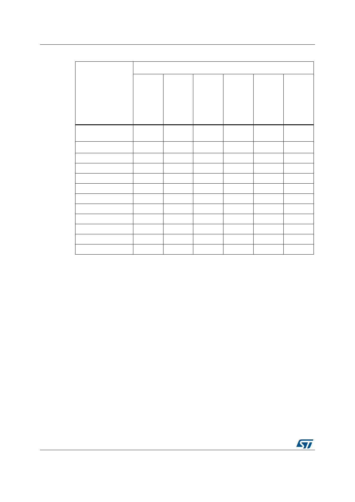
PB3
(JTDO/TRACESWO)
89 133 A10 161 192 C6
PB4 (NJTRST) 90 134 A9 162 193 B7
VSS -----L10
VDD - - - - - K13
BOOT0 94 138 D6 166 197 E8
VCAP3 - - - - - A7
VSS 99 - D5 - 202 L11
PDR_ON - 143 C6 171 203 E7
VDDLDO3 - - - - - A6
VDD 100 144 C5 172 204 L5
VSS -----J16
VDD -----L13
1. PC1, PC13, PC14, PC15 and PI8 are supplied through the power switch. Since the switch only sinks a
limited amount of current (3 mA), the use of GPIOs PC13 to PC15 and PI8 in output mode is limited:
- The speed should not exceed 2 MHz with a maximum load of 30 pF.
- These I/Os must not be used as a current source (e.g. to drive an LED).
2. 5 V tolerant except when in analog mode or oscillator mode for PC14, PC15, PH0 and PH1.
Table 9. Reference connection for all packages (continued)
Pin name (function
after reset)
Pin/ball name
LQFP100
LQFP144
UFBGA176+25
LQFP176
LQFP208
TFBGA240+25
 Loading...


