LED_Anode+
X
Ground
NMI-
X
LAN2 Activity
LED
LED_Anode+
LED_Anode+
LED_Anode+
LED_Anode+
A
B
Power Button
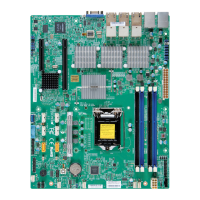
The Power Button connection is located
on pins 1 and 2 of JF1. Momentarily
contacting both pins will power on/off
the system. This button can also be con-
gured to function as a suspend button
(with a setting in the BIOS - See Chapter
5). To turn off the power when the system
is in suspend mode, press the button for
4 seconds or longer. Refer to the table on
the right for pin denitions.
Power Button
Pin Denitions (JF1)
Pin# Denition
1 Signal
2 Ground
Reset Button
Pin Denitions (JF1)
Pin# Denition
3 Reset
4 Ground
A. Reset Button
B. PWR Button
Reset Button
The Reset Button connection is located
on pins 3 and 4 of JF1. Attach it to a
hardware reset switch on the computer
case. Refer to the table on the right for
pin denitions.
A
IPMI CODE
CA
BIOS
LICENSE
BAR CODE
MAC CODE
CA
A
C
A
C
A
+
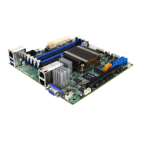
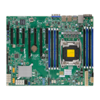
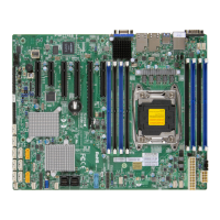
JLAN3
JLAN2
JLAN1
JP1000
JPW1
JPW2
JSTBY1
J4
LE6
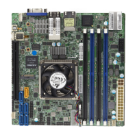
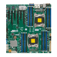
DIMM1
DIMM2
DIMM4
DIMM3
FAN4
FAN3
FAN2
FAN1
FANA
JPME1
JI2C1
JPME2
JI2C2
JPUSB1
JPL1
JPL2
JPL3
JPG1
JBR1
JWD1
JLED1
LE5
LE4
LE1
LE3
J3
JL1
JLED_LAN4
JLED_LAN3
JLED_LAN6
JLED_LAN5
JPI2C1
JTPM1
T-SGPIO1
T-SGPIO2
JSD2
JSD1
SPKR1
B1
JBT1
JF1
SW1
COM1
COM2
PCH SLOT4 PCI-E 2.0 X4(IN X8)
DESIGNED IN USA
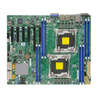
X10SLH-LN6TF
REV:1.01
USB0(3.0)
USB1(3.0)
USB12/13
USB8/9
CPU SLOT6 PCI-E 3.0 X8(IN X16)
I-SATA0
I-SATA2
I-SATA1
I-SATA3
I-SATA4
I-SATA5
VGA
LAN5/6
LAN3/4
LAN1/2
USB4/5 (2.0)
USB2/3(3.0)
JLED1:3 pin Power LED
IPMI LAN
JF1
NIC2
NIC1
ON
PWR
X
RST
OH/
FF
LED
LED
HDD
X
PWR
NMI
C226
X540
X540
X540
BMC
PLX
 Loading...