52
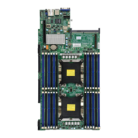
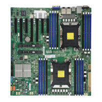
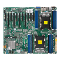
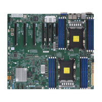
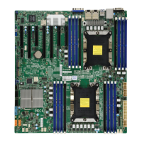
Super X11DPU User's Manual
PSU2
PSU1
X11DPU
DESIGNED IN USA
BAR CODE
IPMI CODE
CPU2
CPU1
BIOS
LICENSE
COM1
LAN
CTRL
LED_P1_D2
LED_P1_D1
LED_P1_E2
LED_P1_E1
LED_P1_F2
LED_P1_F1
LED_P1_A2
LED_P1_A1
LED_P1_C2
LED_P1_B1
LED_P1_B2
LED_P1_C1
LED_P2_F2
LED_P2_F1
LED_P2_E2
LED_P2_E1
LED_P2_D2
LED_P2_D1
LED_P2_C2
LED_P2_C1
LED_P2_B2
LED_P2_B1
LED_P2_A2
LED_P2_A1
JRK1
S-UM12
JVGA2
BT1
JBT1
JL1
JUIDB2
JF1
JPG1
JVRM1
JWD1
FAN8
FAN7
FAN6
FAN5
FAN4
FAN3
FAN2
FAN1
JIPMB1
JNVI2C1
JNVI2C2
SP1
JSD1JSD2
T-SGPIO3
LED1
LEDM1
LEDPWR
JVRM2
JTPM1
SXB3B
SXB1B
SXB2
FAIL
LED
UID NIC
2 1
NIC
LED
HDD PWR
LED
X NMI
PWR
ON
JF1
RST
PS
P2_NVMe1
P2_NVMe0
P2-DIMMF2
P2-DIMMF1
P2-DIMME1
P2-DIMME2
SXB1A
CPU2_PORT3A
CPU2_PORT2C CPU2_PORT2A
SXB1C
P2-DIMMD2
P2-DIMMD1
CPU2_PORT1A
PCH_PORT1 CPU2_DMI
USB3/4 (3.0)
S-SATA0~3
S-SATA4
P2-DIMMA2
S-SATA5
P2-DIMMA1
UID
P2-DIMMB2
P2-DIMMB1
P2-DIMMC2
I-SATA0~3
P2-DIMMC1
I-SATA4~7
GPU PWR2
USB2 (3.0)
P1-DIMMF2
SXB3C
P1-DIMMF1
CPU1_PORT1A
SXB3A
CPU1_PORT3A
CPU1_PORT3C CPU1_PORT2A
CPU1_PORT2C
P1-DIMMD1
P1-DIMME1
P1-DIMME2
P1-DIMMD2
P1-DIMMA2
P1-DIMMA1
P1-DIMMC1
P1-DIMMC2
P1-DIMMB2
P1-DIMMB1
P1_NVMe0 P1_NVMe1
BP PWR4
VGA
IPMI_LAN
USB0/1
(3.0)
BMC
JSDCARD1
PCH
GPU PWR3
GPU PWR4
GPU PWR1
BP PWR2 BP PWR1
BP PWR3
CPU2_PORT3C
JPB1
REV:1.10
JHFI2
JHFI1
T-SGPIO3 Header
A Serial General Purpose Input/Output header (T-SGPIO3) is located on the motherboard.
This header is used to communicate with the enclosure management chip on the backplane.
See the table below for pin denitions.
SGPIO Header
Pin Denitions
Pin# Denition Pin# Denition
1 NC 2 NC
3 Ground 4 DATA Out
5 Load 6 Ground
7 Clock 8 NC
NC = No Connection
Disk-On-Module Power Connector
The Disk-On-Module (DOM) power connectors at JSD1 and JSD2 provide 5V power to a
solid-state DOM storage devices connected to one of the SATA ports. See the table below
for pin denitions.
DOM Power
Pin Denitions
Pin# Denition
1 5V
2 Ground
3 Ground
1
23
1. T-SGPIO3
2. JSD1
3. JSD2
 Loading...