Do you have a question about the Teac V-970X and is the answer not in the manual?
Details the track system, heads, tape type, speed, motors, and wow/flutter.
Specifies frequency response for different tape types and S/N ratios.
Lists dynamic range and fast winding time specifications.
Details input/output, power requirements, consumption, dimensions, and weight.
Provides notes on specifications, improvements, and safety.
Procedure for measuring pinch roller pressure with diagrams.
Procedure and required tools for tape path adjustment.
Connection diagrams for photo sensor adjustment.
Procedure for checking and adjusting reel torque and back tension.
Procedure for adjusting tape speed using a frequency counter.
Methods for measuring wow and flutter during playback and record/playback.
Specifies oils and greases for lubrication after part replacement.
Instructions for converting voltage for general export models.
General precautions for performing electrical checks and adjustments.
List and purpose of TEAC test tapes required for calibration.
Identifies check and adjustment points on the Main PCB (V-970X) and DBX PCB.
Identifies adjustment points on Main PCB (R-919X) and test setup for azimuth.
Procedure for checking and adjusting REC/PLAY head azimuth.
Procedure for checking playback output level.
Procedure for setting the meter level.
Procedure for checking playback frequency response.
Procedure for checking playback signal-to-noise ratio.
Procedures to check minimum and specified line input levels.
Procedures to check meter and headphone output levels.
Procedure for checking the CD level.
Procedure for adjusting bias oscillator frequency and built-in oscillator.
Procedure for setting record equalization and initial bias.
Procedure for adjusting record head azimuth and secondary bias settings.
Procedure for adjusting record level and checking total harmonic distortion.
Checks for built-in oscillator bias and level settings.
Procedures for checking overall frequency response and S/N ratio.
Checks for erase efficiency, REC MUTE function, and channel separation.
Procedure for checking adjacent track crosstalk.
Procedures for adjusting dbx settings and levels.
Notes regarding resistors, capacitors, and safety critical parts.
Detailed exploded view of V-970X components.
List of parts corresponding to Exploded View-1.
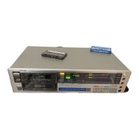
List of accessories included with the product.
Detailed exploded view of V-970X components.
Detailed exploded view of V-970X components.
Detailed exploded view of R-919X components.
List of parts corresponding to Exploded View-4.
Detailed exploded view of R-919X components.
List of parts corresponding to Exploded View-5.
Detailed exploded view of R-919X components.
Diagram and component layout for the V-970X Main PCB.
Diagrams and component layouts for V-970X Joint PCBs C and D.
Diagram and component layout for the R-919X Main PCB.
Diagrams and component layouts for R-919X Joint PCBs C and D.
Diagrams and component layouts for Display PCBs (V-970X and R-919X).
Diagram and component layout for the DBX PCB.
Diagrams for Sensor, Jack, Timer, Power SW, Selector, and Joint PCBs.
Detailed component list for the V-970X Main PCB.
Detailed component list for the R-919X Main PCB.
Detailed component list for the V-970X Main PCB.
Detailed component list for the V-970X Display PCB.
Detailed component lists for V-970X Joint PCBs C and D.
Detailed component list for the R-919X Main PCB.
Detailed component list for the R-919X Display PCB.
Detailed component list for the R-919X Joint PCB C.
Detailed component list for the R-919X Main PCB.
Detailed component list for the R-919X Display PCB.
Detailed component lists for R-919X Joint PCBs C and D.
Component list for the DBX PCB.
Component lists for Power SW and Voltage Selector PCBs.
Component lists for Joint PCBs A and B.
Component lists for Sensor, Jack, and Timer PCBs.
Block diagrams and pin configurations for ICs.
Block diagrams for LM6402H, LA6358, M5220P, LC7800, M4011BP ICs.
Block diagrams for AN6256, BA6209, M51143AL, M5201L, M5218L ICs.
Block diagrams for HA12067NT, CX20187, µPC1297CA, BU4066B ICs.
Block diagrams for AN6256, BA6209, M51143AL, M5201L, M5218L ICs.
Block diagrams for HA12067NT, CX20187, µPC1297CA, BU4066B ICs.
Detailed diagram of V-970X Main PCB with component labels.
Diagrams and component layouts for V-970X Joint PCBs C and D.
Diagrams for R-919X Main, Joint PCBs, Sensor, Jack, Timer, Power SW, Selector.
Circuit schematic for V-970X, showing PCB interconnections.
Circuit schematic for R-919X, showing PCB interconnections.
Circuit schematic for R-919X, showing PCB interconnections.
Circuit schematic for R-919X, showing PCB interconnections.
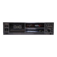
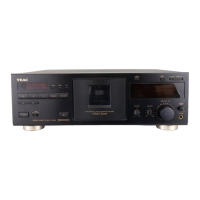
| Type | 3-head, single compact cassette deck |
|---|---|
| Track System | 4-track, 2-channel stereo |
| Tape Speed | 4.76 cm/s |
| Tape Type | type I, CrO2, Metal |
| Frequency Response | 20Hz to 21kHz (Metal tape) |
| Input | 60mV (line) |
| Heads | 1 x erase, 1 x record, 1 x playback |
| Signal to Noise Ratio | 72dB (Dolby C) |
| Wow and Flutter | 0.04% (WRMS) |
| Total Harmonic Distortion | 0.8% |
| Inputs | Line in |
| Outputs | Line out |