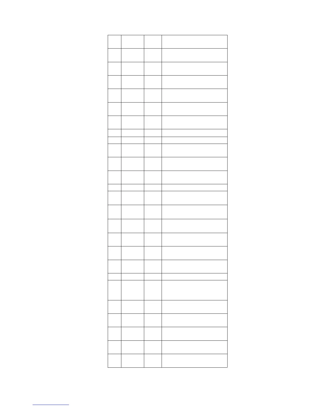
Pin
No.
Mark I/O
Division
Function
18 FOD O Focus drive signal output
terminal
19 TRD O Tracking drive signal
output terminal
20 TVD O Traverse motor drive
signal ouutput terminal
21 SPD O Spindle motor drive signal
output terminal
22 SPON O Drive IC spindle ON signal
output terminal
23 TVON O Drive IC traverse ON signal
output terminal
24
DV
DD
0
I Power supply terminal
25 FG I FG input terminal
26 NRECT O Rec/Play switching signal
output terminal
27 IVDD2 — Power supply terminal for
I/O pad
28 IVDD0 — Power supply terminal for
I/O pad
29 DVss0 — GND terminal
30
~32
RAD12
~RAD10
— DRAM address output
terminal (Not used, open)
33
~42
RAD9
~RAD0
O DRAM address output
terminal
43
~46
RDT3
~RDT0
I/O DRAM data input/output
terminal
47 NRAS O DRAM row address strobe
output terminal
48 NCAS O DRAM culum address
strobe output terminal
49 NWE O DRAM write enable output
terminal
50 NRST I Reset signal input terminal
51 SELAD I MSP/MDA,I/F address
select input terminal (“H”
Address)
52 SSCK I MSP/MDA,I/F clock input
terminal
53 SSDW I MSP/MDA,I/F write data
input terminal
54 SSDR O MSP/MDA,I/F read data
output terminal
55 MDISY O Leader synchronous signal
output
56 SCTSY O ADIP synchronous noise
output terminal
42