WE866E4-P Module Hardware User Guide
1VV0301487 Rev. 1.2 28 2018-07-27
PRELIMINAR
Y
6.4.1 PCB Design Guidelines
The WE866E4-P module provides a 50Ω antenna pad, which is routed to the antenna
connector (or the integrated antenna) by means of a transmission line.
It is important that the impedance of this line is controlled to 50Ω. The line should be as
short as possible with a constant cross section and without abrupt curves. It is isolated from
any other noise sources and cross overs from other lines in adjacent layers. Instead, a
continuous ground plane is recommended under the antenna trace and a ground via curtain
should connect to the coplanar ground planes.
An example of implementation - the details of the antenna trace on the WE866E4-P
interface board is as described:
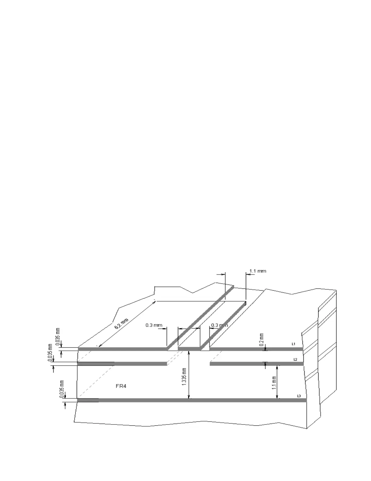
A Grounded Coplanar Waveguide (G-CPW) line has been chosen, since this kind of
transmission line ensures good impedance control and can be implemented in an outer PCB
layer as required in this case. A SMA female connector has been used to feed the line.
The interface board is realized on a FR4, 4-layers PCB. Substrate material is characterized
by relative permittivity εr = 4.6 ± 0.4 @ 1 GHz, TanD= 0.019 ÷ 0.026 @ 1 GHz.
A characteristic impedance of nearly 50 Ω is achieved using trace width of 1.1 mm,
clearance from coplanar ground plane = 0.3 mm each side. The line uses reference ground
plane on layer 3, while copper is removed from layer 2 underneath the line. Height of the
trace above ground plane is 1.335 mm. Calculated characteristic impedance is 51.6 Ω,
estimated line loss is less than 0.1 dB.
Figure 2, page 28 shows the line geometry:
Figure 2 PCB Design