WE866E4-P Module Hardware User Guide
1VV0301487 Rev. 1.2 39 2018-07-27
PRELIMINAR
Y
9.3.1 Recommendations for PCB Pad Surface
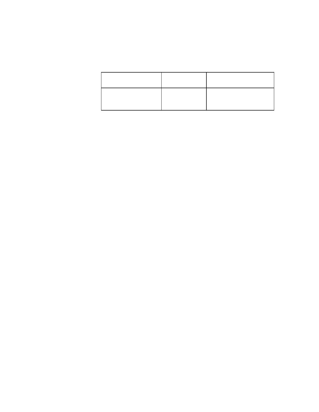
Table 17, page 39 provides the recommendation for PCB Pad Surface.
The PCB must be able to resist higher temperatures which occurs at the lead-free process.
This issue should be discussed with the PCB supplier. Generally, the wettability of tin-lead
solder paste on the described surface plating is better compared to lead-free solder paste.
It is not necessary to panel the application PCB, however it is suggested to use milled
contours and pre-drilled board breakouts. Scoring or v-cut solutions are not recommended.
9.4 Stencil
Stencil’s apertures layout can be the same of the recommended footprint (1:1), a thickness
of stencil foil ≥ 120 μm is suggested.
9.5 Solder Paste
It is recommended to use only “no clean” solder paste in order to avoid the cleaning of the
modules after assembly. The lead-free solder paste is Sn/Ag/Cu.
9.6 Solder Re-flow
Figure 11, page 40 shows the recommended solder profile re-flow:
Table 17 Recommendation for PCB Pad Surface
Finish Layer Thickness
(um)
Properties
Electro-less
Ni/Immersion Au
3 - 7/ 0.03 - 0.15
Good solderability
protection, high shear force
values