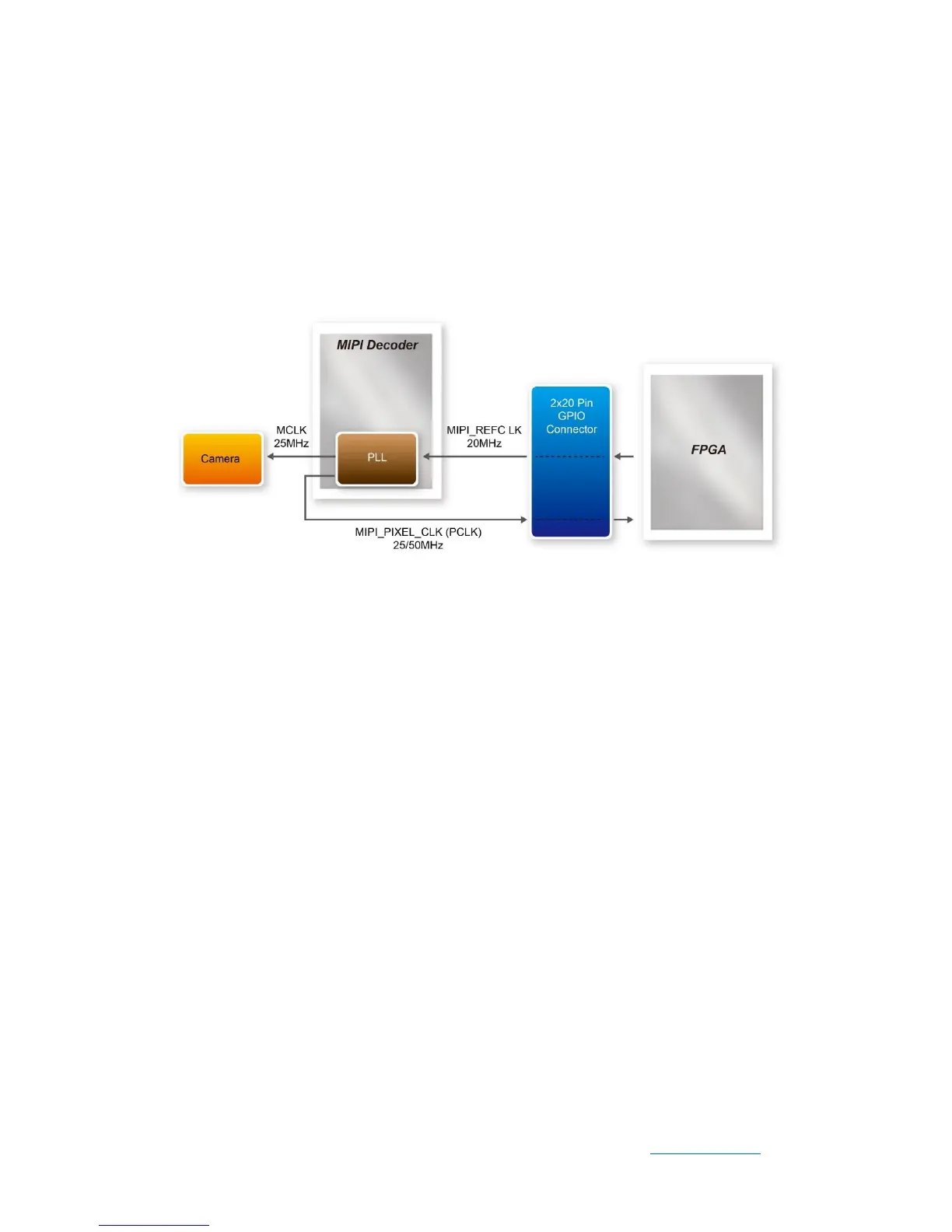
3.4 Clock Tree
Figure 3-5 is the D8M board clock tree block diagram. MIPI Decoder PLL receives
FPGA Reference Clock (MIPI_REFCLK) and outputs Clock to Camera sensor (MCLK),
at the same time, MIPI Decoder PLL will also output a parallel port clock
(MIPI_PIXEL_CLK) and feedback to the FPGA to deal with parallel data.
Figure 3-5 Simple Clock Tree of the D8M Board
In the provided demonstrations, MIPI_REFCLK is set to 20MHz, FPGA transmits this
clock to the D8M MIPI Decoder PLL through the GPIO connector. No matter how much
the camera resolution is, the MCLK fixed output is 25MHz. According to the output
resolution, MIPI_PIXEL_CLK can be set as 25MHz for 640x480@60fps and 50MHz for
1920x1080@15fps.
For more MIPI Decoder PLL setting details, please refer to
TC358746AXBG_748XBG_rev09.pdf "Chapter 5: Clock and System" or refer to
Terasic demonstrations.
3.5 Camera Configuration
The developers should configure the camera OV8865 via I2C so the camera can
output desired image format. To get a better image quality, the following register
settings are strongly recommended. These settings are all applied in the CD demo
code. For detail information about the registers, please refer the OV8865 datasheet
included in the System CD.
 Loading...