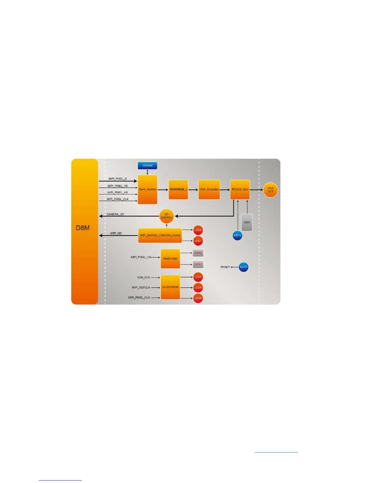
Figure 4-4 is the function block diagram of this demonstration. This design block is
similar to Line-Buffer’s. The only difference is one more Sdram_Control module is
there. This module can control general external SDRAM Memory and read/write image
data. As shown in the block diagram, D8M raw data will be written in SDRAM first. After
finishing writing a Frame, Sdram_Control module will read out the data from SDRAM to
RAW2RGB_J module to convert RAW data to RGB data. The RGB data will output
along with the signal timing generated by VGA_Controller to VGA monitor.
In the block, other module (for example, FOCUS_ADJ,
MIPI_BRIDGE_CAMERA_Config, FpsMonitor, CLOCKMEM) function instructions and
KEY/SW operations are the same with Line-Buffer’s:
Figure 4-4 Block diagram of the digital camera D8M design with Frame -Buffer
We provide the Frame-Buffer demonstrations on both DE1-SoC and DE2-115. And the
display resolution is 640x480@60Hz too. The demonstration setting up methods are
the same with section 4.1.Please see following instructions for details.
DE1-SoC Demonstration:
◼ Design Tools
⚫ Quartus II v15.0
◼ Demonstration Source Code
 Loading...