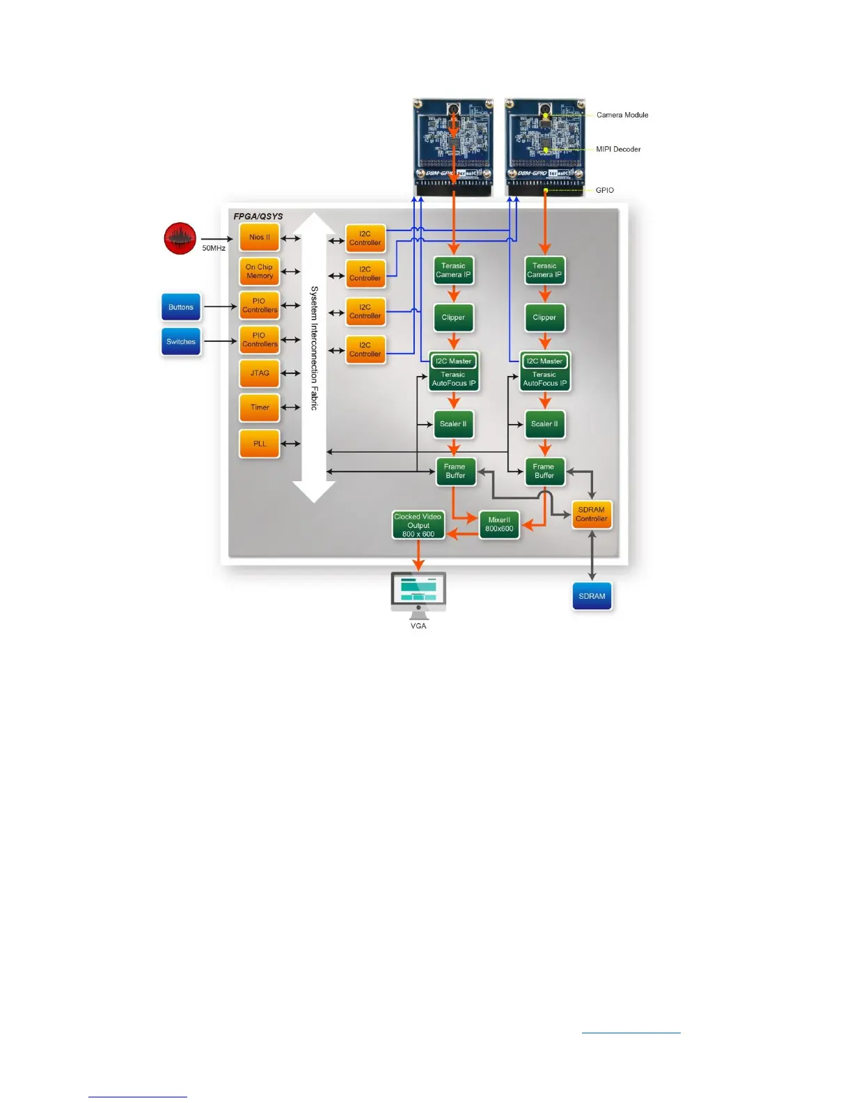
Figure 5-4 Function block diagram of DE1_SOC_D8MX2_VIP demonstration
DE1_SOC_D8MX2_VIP reference design is developed based on Altera’s Video and
Image Processing (VIP) suite. This demo implements two D8M boards and outputs
their parallel images data into the FPGA. Insside the FPGA, image data will enter the
Terasic Camera IP, Cliper, Terasic AutoFocus and Scaller blocks sequentially. After that,
10bit RAW data will be converted to 24-bit RGB data (in 640x480 resolution) and
stored into the SDRAM as a cache via the Frame Buffer block. Then, these two image
streams will be read and blended together (in 800x600 resolution) by Mixer IP. Finally it
displays on the VGA monitor via Clock Video Output block.
The Nios II program running the on-chip memory controls on the two I2C controllers to
configure the image sensor, motor driver, and the MIPI CSI-2 Decoder IC.
Note: The focus driver IC (VM149C) in the camera module is also configured by the
 Loading...