~----9_4_5_42_4_-9_7_0_1
__________________________________________________
_
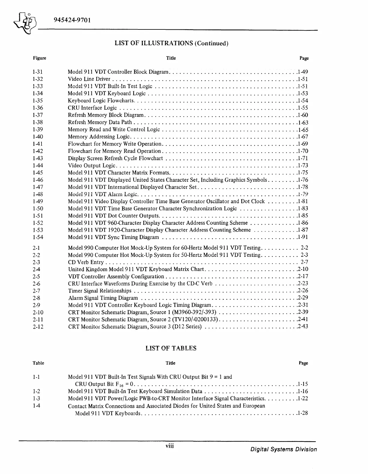
LIST
OF
ILLUSTRATIONS (Continued)
Figure
Title Page
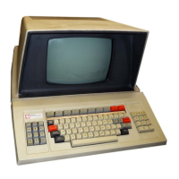
1-31 Model 911 VDT Controller Block Diagram
....................................
.1-49
1-32 Video Line Driver
.....................................................
1-51
1-33 Model 911 VDT
Built~In
Test Logic
.........................................
1-51
1-34 Model 911 VDT Keyboard Logic
...........................................
1-53
1-35 Keyboard Logic Flowcharts
..............................................
.1-54
1-36 CRU Interface Logic
..................................................
.1-55
1-37 Refresh Memory Block Diagram
............................................
1-60
1-38 Refresh Memory Data
Path
...............................................
1-63
1-39 Memory Read and Write Control Logic
.......................................
1-65
1-40 Memory Addressing Logic
...............................................
.1-67
1-41 Flowchart for Memory Write Operation
......................................
.1-69
1-42 Flowchart for Memory Read Operation
......................................
.1-70
1-43 Display Screen Refresh Cycle Flowchart
.....................................
.1-71
1-44 Video
Output
Logic
....................................................
1-73
1-45 Model 911 VDT Character Matrix Formats
....................................
.1-75
1-46 Model 911 VDT Displayed United States Character Set, Including Graphics Symbols
.........
1-7
6
1-47 Model 911 VDT International Displayed Character
Set.
...........................
.1-78
148
Model 911 VDT Alarm Logic
.............................................
. l-79
1-49 Model 911 Video Display Controller Time Base Generator Oscillator and Dot Clock
........
.1-81
1-50 Model 911 VDT Time Base Generator Character Synchronization Logic
................
.1-83
1-51 Model 911 VDT
Dot
Counter
Outputs
.......................................
.1-85
1-52 Model
911VDT960-Character
Display Character Address Counting Scheme
.............
.1-86
1-53 Model 911 VDT 1920-Character Display Character Address Counting Scheme
............
.1-87
1-54 Model 911 VDT Sync Timing Diagram
......................................
.1-91
2-1
Model
990
Computer Hot Mock-Up System for 60-Hertz Model 911 VDT Testing
...........
2-2
2-2 Model
990
Computer Hot Mock-Up System for 50-Hertz Model 911 VDT Testing
...........
2-3
2-3 CD Verb
Entry
.......................................................
2-7
2-4 United Kingdom Model 911 VDT Keyboard Matrix Chart
...........................
2-10
2-5 VDT Controller Assembly Configuration
......................................
2-17
2-6 CRU Interface Waveforms During Exercise
by
the
CD-C
Verb
........................
2-23
2-7 Timer Signal Relationships
...............................................
2-26
2-8 Alarm Signal Timing Diagram
............................................
.2-29
2-9 Model 911 VDT Controller Keyboard Logic Timing Diagram
.........................
2-31
2-10 CRT Monitor Schematic Diagram, Source 1 (M3960-392/-393)
.......................
2-39
2-11 CRT Monitor Schematic Diagram, Source 2 (TV120/-0200133)
.......................
2-41
2-12 CRT Monitor Schematic Diagram, Source 3 (D12 Series)
..........................
.
243
Table
1-1
1-2
1-3
1-4
L!ST
OF
TA.BLES
Title
Page
Model 911 VDT Built-In Test Signals With CRU
Output
Bit 9 = 1 and
CRU
Output
Bit F
16
= 0
..............................................
.1-15
Model 911 VDT Built-In Test Keyboard Simulation Data
..........................
.1-16
Model 911 VDT Power/Logic PWB-to-CRT Monitor Interface Signal Characteristics
.........
.1-22
Contact Matrix Connections and Associated Diodes for United States and European
Model 911 VDT Keyboards
............................................
.1-28
viii
Digital
Systems Division