2.2 Power
The LP-EM-CC35X1 is designed to accept power from a connected LP-XDS110 and an external USB-C power
connection together.
WARNING
To verify proper functioning of the board, the LP-XDS110 and USB-C power cable from the LP-EM-
CC35X1 must be connected to the same computer. Do not connect the USB-C cable to a wall outlet
or different computer.
The use of Schottky diodes make sure that load sharing occurs between the USB connectors on the LaunchPad
kit and the BoosterPack module without any board modifications. The jumpers labeled J14 (1.8V) and J13 (3.3V)
can be used to measure the total current consumption of the board from the onboard LDO.
2.2.1 VIO Selection
The CC35xxE device features three Voltage IO rings (VIOs) for choosing the reference voltage of the various
IOs. These three VIOs are VIO1, VIO2, and VDDSF. Each one the IO rings can be set to 1.8V or 3.3V
independently of each other.
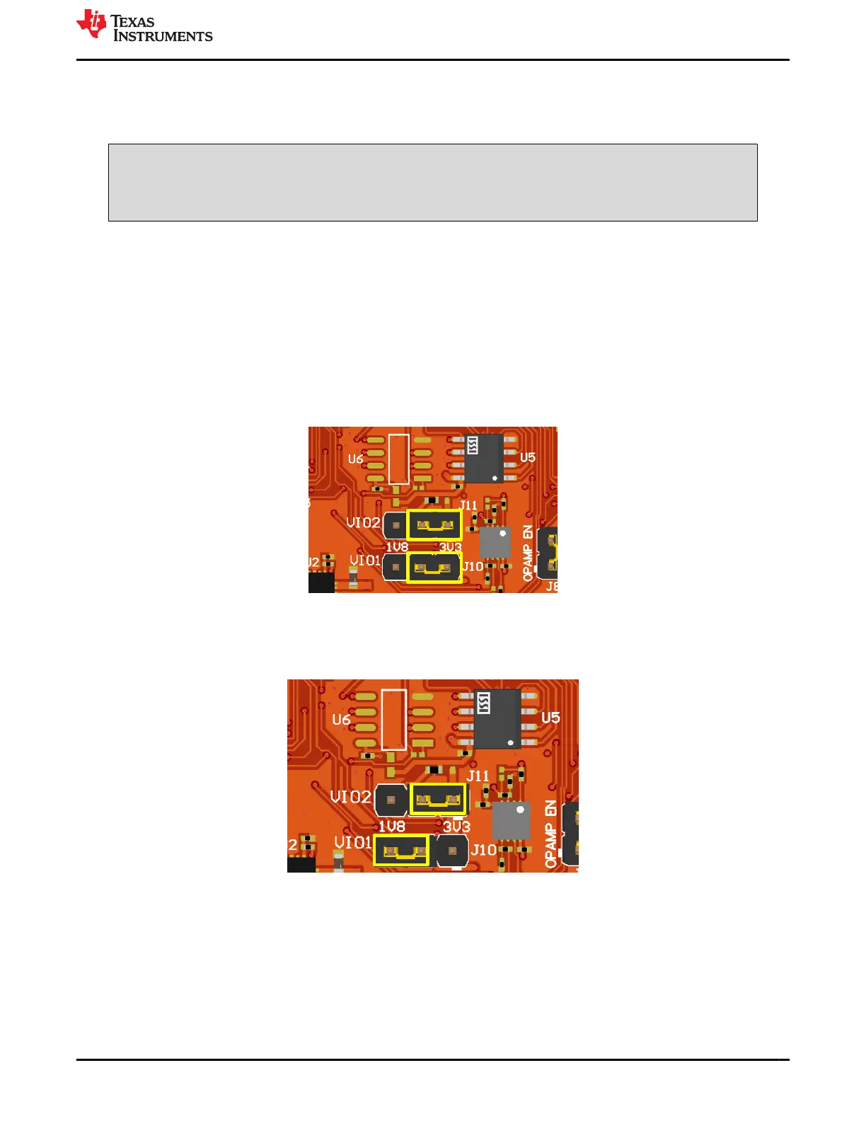
The LP-EM-CC35X1 features 2 jumpers (J10, J11) for easy voltage configuration for VIO1 and VIO2, either to
1.8V or 3.3V. By default both are set to 3.3V; see Figure 2-20.
Figure 2-20. VIO Jumpers
To set either VIO to 1.8V instead of 3.3V, place the jumper on the left two header pins. For example, VIO1 is set
to 1.8V and VIO2 is set to 3.3V as shown in Figure 2-21.
Figure 2-21. VIO Selection Example
VDDSF IO ring controls the reference voltage of the xSPI signals to the external flash and PSRAM. For more
information on VDDSF, see Section 2.1.5.
For the VIO selection of each GPIO, see Table 2-8.
www.ti.com Hardware
SWRU629 – SEPTEMBER 2024
Submit Document Feedback
CC35xxE LaunchPad™ Development Kit for SimpleLink™ Wi-Fi 6 and
Bluetooth® Low Energy Wireless MCU
17
Copyright © 2024 Texas Instruments Incorporated