2.1 Wired Connections, Jumper Settings, Buttons, and LEDs
2.1.1 SWD Interface
The LP-EM-CC35X1 supports Serial Wire Debug (SWD) interface to an external XDS110 or other JTAG-based
debuggers. The SWD interface to the CC35xxE device is used for flashing the device and basic debugging. The
SWD lines are part of the VIO1 IO ring, the voltage of which can be controlled by shunt J10, see Section 2.2.1 .
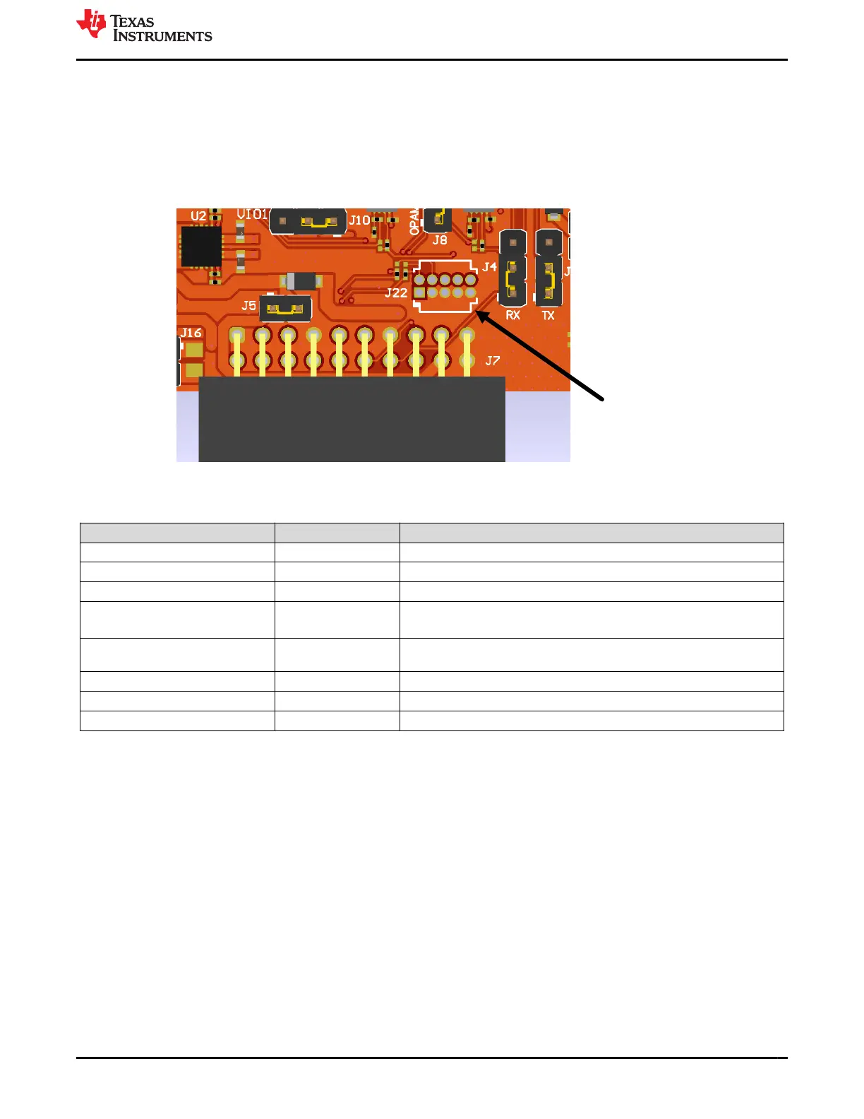
The default SWD connection is to the LP-XDS110 20-pin header on the bottom of the LP-EM-CC35X1 (J7).
Footprint for Arm
10-pin JTAG
connector
Figure 2-2. SWD Interfaces
Table 2-1. 20 pin LP-XDS110 Connector Assignment
Pin Signal Name Description
J7.6 SWCLK Serial wire clock
J7.8 SWDIO Serial wire data in/out
J7.10 XDS_RESET nRESET (enable line to the CC3551E)
J7.12 UART1_TX_XDS The CC3551E UART TX (from CC3551E)
(can be disconnected with jumpers; see Section 2.1.3)
J7.14 UART1_RX_XDS The CC3551E UART RX (to CC3551E) (can be disconnected with jumpers;
see Section 2.1.3)
J7.16 VIO1 VIO1 supply reference voltage to connector
J7.18 VCC_BRD_5V 5V supply to LP-EM-CC35X1 from LP-XDS110
J7.1, J7.7, J7.13, J7.19, J7.20 GND Board ground
www.ti.com Hardware
SWRU629 – SEPTEMBER 2024
Submit Document Feedback
CC35xxE LaunchPad™ Development Kit for SimpleLink™ Wi-Fi 6 and
Bluetooth® Low Energy Wireless MCU
5
Copyright © 2024 Texas Instruments Incorporated