www.ti.com
PLL Loop Filters and Loop Parameters
9
SNAU145B–MAY 2013–Revised March 2018
Submit Documentation Feedback
Copyright © 2013–2018, Texas Instruments Incorporated
LMK04826 and LMK04828 User’s Guide
3 PLL Loop Filters and Loop Parameters
In jitter cleaning applications that use a cascaded or dual PLL architecture, the first PLL’s purpose is to
substitute the phase noise of a low-noise oscillator (VCXO or crystal resonator) for the phase noise of a
“dirty” reference clock. The first PLL is typically configured with a narrow loop bandwidth to minimize the
impact of the reference clock phase noise. The reference clock consequently serves only as a frequency
reference rather than a phase reference.
The loop filters on the LMK048xx evaluation board are setup using the approach above. The loop filter for
PLL1 has been configured for a narrow loop bandwidth (> 100 kHz). The specific loop bandwidth values
depend on the phase noise performance of the oscillator mounted on the board. Table 2 and Table 3
contain the parameters for PLL1 and PLL2 for each oscillator option.
TI’s Clock Design Tool can be used to optimize PLL phase noise/jitter for given specifications. See:
http://www.ti.com/tool/clockdesigntool.
3.1 PLL1 Loop Filter
(1)
Loop Bandwidth is a function of Kφ, Kvco, N as well as loop components. Changing Kφ and N will change the loop bandwidth.
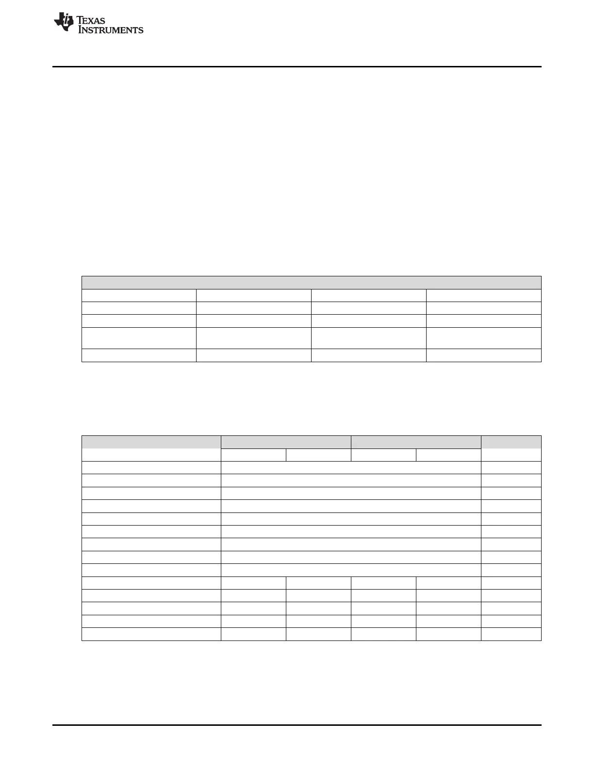
Table 2. PLL1 Loop Filter Parameters for Crystek 122.88 MHz VCXO
(1)
122.88 MHz VCXO PLL
Phase Margin 50˚ Kφ (Charge Pump) 150 µA
Loop Bandwidth 14 Hz Phase Detector Freq 1.024 MHz
VCO Gain 2.0 kHz/V
Reference Clock Frequency 122.88 MHz Output Frequency 122.88 MHz
(To PLL 2)
Loop Filter Components C1_A1 = 100 nF C2_A1 = 680 nF R2_A1 = 39 kΩ
3.2 PLL2 Loop Filter
(1)
PLL Loop Bandwidth is a function of Kφ, Kvco, N as well as loop components. Changing Kφ and N will change the loop
bandwidth.
Table 3. Integrated VCO PLL
(1)
LMK04826 LMK04828
VCO0 VCO1 VCO0 VCO1
C1_A2 0.047 nF
C2_A2 3.9 nF
C3 (internal) 0.01 nF
C4 (internal) 0.01 nF
R2_A2 0.62 kΩ
R3 (internal) 0.2 kΩ
R4 (internal) 0.2 kΩ
Charge Pump Current, Kφ 3.2 mA
Phase Detector Frequency 122.88 MHz
Frequency 1966.08 2457.6 2457.6 2949.12 MHz
Kvco 15.3 8.9 21.9 17.4 MHz/V
N 16 20 20 24
Phase Margin 73 64 73 70 degrees
Loop Bandwidth 303 151 344 233 kHz