EasyManua.ls Logo

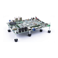
Texas Instruments Jacinto7 J721E - User Manual

Texas Instruments Jacinto7 J721E
85 pages
To Next Page IconTo Next Page
Loading...
1
SPRUIS4ADecember 2019Revised May 2020
Submit Documentation Feedback
Copyright © 2019–2020, Texas Instruments Incorporated
Jacinto7 J721E/DRA829/TDA4VM Evaluation Module (EVM)
User's Guide
SPRUIS4ADecember 2019Revised May 2020
Jacinto7 J721E/DRA829/TDA4VM Evaluation Module
(EVM)
This technical user's guide describes the hardware architecture and configuration options of the
J721E/DRA929/TDA4VM EVM.
Contents
1 Introduction ................................................................................................................... 5
1.1 Key Features ........................................................................................................ 5
1.2 Thermal Compliance ............................................................................................... 6
1.3 REACH Compliance................................................................................................ 7
2 J721E EVM Overview....................................................................................................... 7
2.1 J721E EVM Board Identification.................................................................................. 9
2.2 J721E SOM Component Identification ......................................................................... 10
2.3 Jacinto7 Common Processor Components Identification .................................................... 11
2.4 Quad Ethernet Components Identification ..................................................................... 12
3 EVM User Setup/Configuration........................................................................................... 13
3.1 Power Requirements.............................................................................................. 13
3.2 Power ON Switch and Power LEDs ............................................................................ 14
3.3 EVM Reset/Interrupt Push Buttons ............................................................................. 18
3.4 EVM DIP Switches ................................................................................................ 19
3.5 EVM UART/COM Port Mapping................................................................................. 23
3.6 JTAG Emulation ................................................................................................... 24
4 J721E EVM Hardware Architecture...................................................................................... 27
4.1 J721E EVM Hardware Top level Diagram ..................................................................... 27
4.2 J721E EVM Interface Mapping.................................................................................. 29
4.3 I2C Address Mapping............................................................................................. 30
4.4 GPIO Mapping..................................................................................................... 31
4.5 Power Supply ...................................................................................................... 32
4.6 Reset ............................................................................................................... 38
4.7 Clock ............................................................................................................... 40
4.8 Memory interfaces................................................................................................. 43
4.9 MCU Ethernet Interface .......................................................................................... 49
4.10 QSGMII Ethernet Interface....................................................................................... 51
4.11 PCIe Interface ..................................................................................................... 53
4.12 USB Interface...................................................................................................... 59
4.13 CAN Interface...................................................................................................... 62
4.14 FPD Interface (Audio Deserializer).............................................................................. 65
4.15 FPD Panel Interface (DSI Video Serializer) ................................................................... 66
4.16 Display Serial Interface (DSI) FPC.............................................................................. 67
4.17 Audio Interface .................................................................................................... 67
4.18 Display Port Interface ............................................................................................ 69
4.19 MLB Interface ..................................................................................................... 69
4.20 I3C Interface ...................................................................................................... 71
4.21 ADC Interface ..................................................................................................... 71
4.22 RTC Interface ..................................................................................................... 72
4.23 Apple Authentication Header .................................................................................... 73
4.24 EVM Expansion Connectors..................................................................................... 74

Table of Contents

Question and Answer IconNeed help?

Do you have a question about the Texas Instruments Jacinto7 J721E and is the answer not in the manual?

Texas Instruments Jacinto7 J721E Specifications

General IconGeneral
BrandTexas Instruments
ModelJacinto7 J721E
CategoryMotherboard
LanguageEnglish

Summary

Introduction

1.1 Key Features

Highlights the main features of the J721E EVM platform.

1.2 Thermal Compliance

Discusses thermal considerations and cautions for the EVM.

1.3 REACH Compliance

Details the EVM's compliance with EU REACH regulations.

J721 E EVM Overview

2.1 J721 E EVM Board Identification

Identifies the main boards of the J721E EVM system.

2.2 J721 E SOM Component Identification

Identifies key components on the J721E SOM board.

2.3 Jacinto7 Common Processor Components Identification

Identifies components on the Common Processor Board.

2.4 Quad Ethernet Components Identification

Identifies components of the Quad Ethernet Expansion Board.

EVM User Setup;Configuration

3.1 Power Requirements

Specifies the power supply requirements for the EVM.

3.2 Power ON Switch and Power LEDs

Explains how to use the power switch and interpret power LEDs.

3.3 EVM Reset;Interrupt Push Buttons

Details the function of reset and interrupt push buttons.

3.4 EVM DIP Switches

Describes the function of EVM configuration DIP switches.

3.4.1 EVM Configuration DIP Switch

Details EVM configuration settings using DIP switch SW3.

3.4.2 SOM Configuration DIP Switch

Details SOM configuration settings using DIP switches SW1-SW3.

3.4.3 Boot Modes

Explains how to set boot modes using DIP switches SW8 and SW9.

3.5 EVM UART;COM Port Mapping

Maps UART ports to COM ports and FTDI bridges.

3.6 JTAG Emulation

Describes JTAG emulation setup and multiplexing.

J721 E EVM Hardware Architecture

4.1 J721 E EVM Hardware Top level Diagram

Shows the overall functional block diagram of the J721E EVM.

4.2 J721 E EVM Interface Mapping

Maps EVM interfaces to SoC ports and device part numbers.

4.3 I2 C Address Mapping

Lists I2C devices and their assigned addresses on the EVM.

4.4 GPIO Mapping

Details the mapping of SoC GPIOs to EVM peripherals.

4.5 Power Supply

Explains the power distribution system for the J721E SOM.

4.5.1 Power Sequencing

Illustrates the power-up sequence of EVM power supplies.

4.5.2 Voltage Supervisor

Describes the voltage supervisor circuits for monitoring power rails.

4.5.3 DDR I;O Voltage Selection

Explains how to select DDR/LPDDR4 I/O voltage using DIP switches.

4.5.3.1 J721 E SoC S2 R Logic Flow

Steps to enter Suspend-to-RAM (S2R) low power state.

4.5.3.2 J721 E SoC MCU Only Operation

Steps for MCU Only low power state operation.

4.5.3.3 Power Monitoring

Details the INA devices used for power monitoring.

4.6 Reset

Explains the EVM reset architecture and sources.

4.7 Clock

Describes the clock architecture of the J721E EVM.

4.7.1 Processors Primary Clock

Details the primary clock sources for the J721E processor.

4.7.2 Processors Secondary;SERDES Ref Clock

Explains secondary and SERDES reference clocks.

4.7.3 EVM Peripheral Ref Clock

Describes reference clocks for EVM peripherals.

4.8 Memory interfaces

Covers various memory interfaces on the J721E EVM.

4.8.1 LPDDR4 Interface

Details the LPDDR4 memory interface.

4.8.2 OSPI Interface

Details the OSPI and Hyper Flash memory interface.

4.8.3 UFS Interface

Details the UFS flash memory interface.

4.8.4 MMC Interface

Covers MMC interfaces including eMMC and Micro SD.

4.8.4.1 MMCO - eMMC Interface

Details the eMMC flash interface.

4.8.4.2 MMC1 - Micro SD Interface

Details the Micro SD card interface.

4.8.5 Board ID EEPROM Interface

Describes the Board ID EEPROM interface for identification.

4.8.6 Boot EEPROM Interface

Details the Boot EEPROM interface for booting.

4.9 MCU Ethernet Interface

Explains the MCU Gigabit Ethernet interface.

4.9.1 Gigabit Ethernet PHY Default Configuration

Configuration details for the Gigabit Ethernet PHY.

4.10 QSGMII Ethernet Interface

Describes the Quad SGMII Ethernet interface.

4.11 PCle Interface

Covers the PCIe interfaces on the EVM.

4.11.1 X1 Lane PCle Interface

Details the X1 lane PCIe interface.

4.11.2 X2 Lane PCle Interface

Details the X2 lane PCIe interface.

4.11.3 M.2 PCIe Interface

Details the M.2 PCIe interface.

4.12 USB Interface

Explains the USB interfaces available on the EVM.

4.12.1 USB 3.1 Interface

Details the USB 3.1 Type C interface.

4.12.2 USB 2.0 Interface

Details the USB 2.0 Hub interface.

4.12.3 USB 3.0 Micro AB Interface (Reserved Port)

Notes the reserved USB 3.0 Micro AB interface.

4.13 CAN Interface

Details the CAN interfaces supported by the EVM.

4.14 FPD Interface (Audio Deserializer)

Describes the FPD Link III Audio Deserializer interface.

4.15 FPD Panel Interface (DSI Video Serializer)

Describes the DSI to FPD Link III Serializer interface.

4.16 Display Serial Interface (DSI) FPC

Explains the DSI FPC interface for display panels.

4.17 Audio Interface

Details the Audio Codec interface and port mapping.

4.18 Display Port Interface

Describes the Display Port interfaces (DP0 and DP1).

4.19 MLB Interface

Details the Media Local Bus (MLB) interface.

4.20 I3 C Interface

Explains the I3C interfaces for MCU and MAIN domains.

4.21 ADC Interface

Describes the ADC interface and its connector.

4.22 RTC Interface

Details the Real-Time Clock (RTC) module.

4.23 Apple Authentication Header

Describes the provision for Apple authentication interface.

4.24 EVM Expansion Connectors

Details the expansion connectors for add-on boards.

4.25 ENET Expansion Connector

Describes the ENET expansion connector and its features.

4.25.1 Power requirements

Specifies power requirements for the ENET expansion card.

4.25.2 Clock

Details clock sources for the ENET expansion board.

4.25.2.1 Main Clock

Describes the main clock for the PHY on the ENET expansion board.

4.25.2.2 Optional Clock

Discusses the optional clock source for the ENET expansion board.

4.25.3 Reset Signals

Explains the reset signals for the ENET expansion connector.

4.25.4 Ethernet Interface

Details the SGMII Ethernet interface on the expansion board.

4.25.4.1 Quad Port SGMII PHY Default Configuration

Configuration for the Quad Port SGMII PHY.

4.25.5 Board ID EEPROM Interface

Describes the Board ID EEPROM on the ENET expansion board.

4.26 CSI Expansion Connector

Details the CSI expansion connectors for camera modules.

Related product manuals