Mode SEL0: 3
Mode SEL1: 4
Splitter = 0, DSI lanes = 4
Non–Cont. Clk = 1, Coax = 0,
STP, DSI Disable = 0
7b’ I2C Address
0x16 (default)
R1 R2
16.2K
40.2K
(other – see DM)
“R3”
“R4”
“R5”
“R6”
See “R1” in table
See “R2” in table
MODE Selection DEVICE ALIAS ID
J721E EVM Hardware Architecture
www.ti.com
66
SPRUIS4A–December 2019–Revised May 2020
Submit Documentation Feedback
Copyright © 2019–2020, Texas Instruments Incorporated
Jacinto7 J721E/DRA829/TDA4VM Evaluation Module (EVM)
Table 34 lists the pinout for the HSD connector J1.
Table 34. FPD Audio Deserializer HSD Connector Pinout
Pin No Signal
1 GND
2 RIN_N
3 POWER (12V)
4 RIN_P
4.15 FPD Panel Interface (DSI Video Serializer)
CP Board supports TI ‘s DSI to FPD Link III Serializer IC Mfr. Part# PDS90UB941ASRTDTQ1.
DSI0 port of J721E SOC shall be connected to DSI to FPD-Link III serializer bridge and FPD Link-III
signals are terminated to HSD connector of Mfr. Part# D4S20G-400A5-C to interface with display panel.
Reference clock to the FPD bridge is provided from Peripheral clock generator (CDCEL) and onboard
clock oscillator ASDMB-25.000MHZ-XY-T with the resistor option. The default clock source is selected to
onboard clock oscillator.
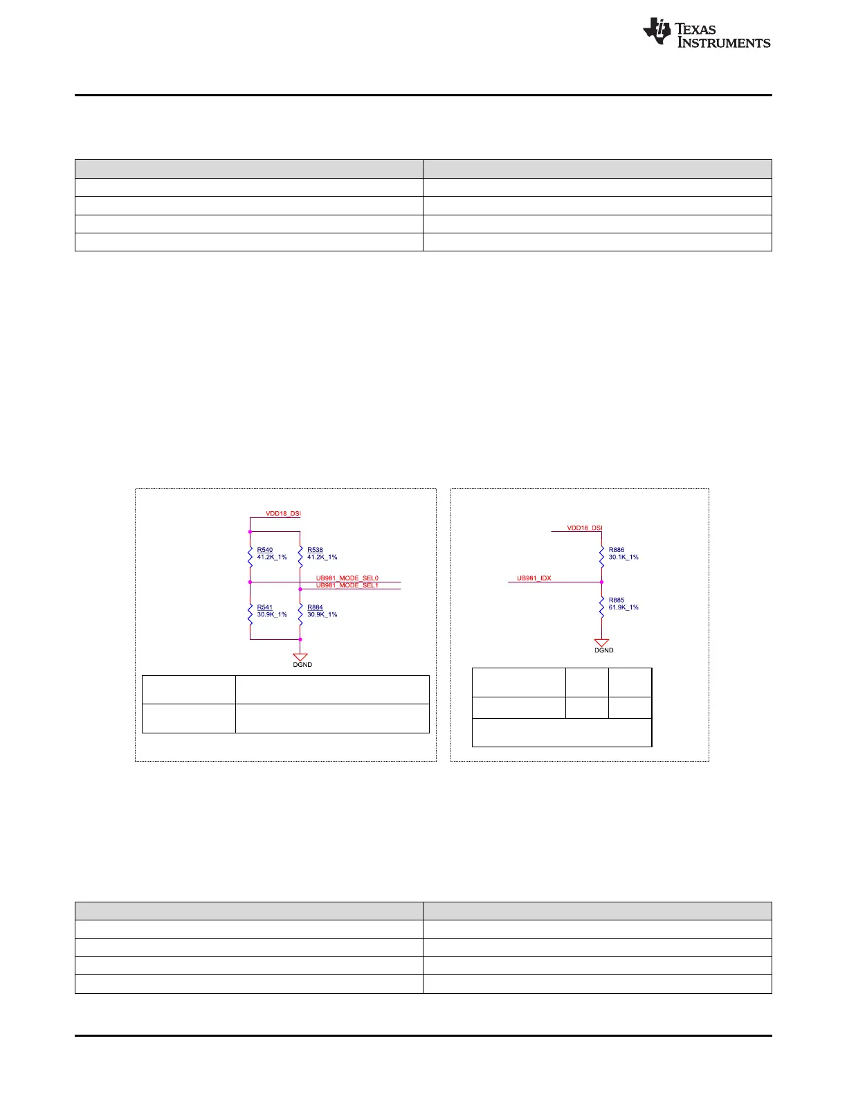
The I2C1 signals of J721E being used for controlling of the FPD bridge. A 30.1KΩ pull up and 61.9KΩ pull
down is provided on ID[X] pin to set the 7‘b I2C address to 0x16.
The device Alias ID and the Mode selection is set by hardware strap resistors, as shown in Figure 51.
Figure 51. FPD-Link UB981 Device Settings Circuit
Power +12 V is provided to the HSD connector using a power switch TPS1H100AQPWPRQ1 to power the
display panel. The power switch is controlled by a GPIO expander signal (PWR_SW_CNTL_DSI0).
Table 35 lists the pinout for the HSD connector J45.
Table 35. DSI to FPD Serializer HSD Connector Pinout
Pin No Signal
1 DOUT0_P
2 POWER (12V)
3 DOUT0_N
4 GND