J721E EVM Hardware Architecture
www.ti.com
42
SPRUIS4A–December 2019–Revised May 2020
Submit Documentation Feedback
Copyright © 2019–2020, Texas Instruments Incorporated
Jacinto7 J721E/DRA829/TDA4VM Evaluation Module (EVM)
4.7.2 Processor’s Secondary/SERDES Ref Clock
In addition to the Primary clock, the SERDES reference clocks to the SoC is sourced from the Clock
Generator (CDCI6214) on the Common processor board. All these clocks are 100 MHz with HCSL level
for the SoC’s SERDES reference clock input. The programming of CDCI6214 chip is done through J721E
SoC’s I2C0 port.
There are two CDCI6214 clock generators available to source the SERDES reference clocks to SoC. The
CDCI1 (U22) is not connected to I2C0 port by default. The clocks from CDCI1 (U22) is derived using
factory programmed configuration.
Only the CDCI2 (U17) is required I2C programming for the desired clock outs from each channel. A 25
MHz crystal is attached the each CDCI chip for its reference clock inputs.
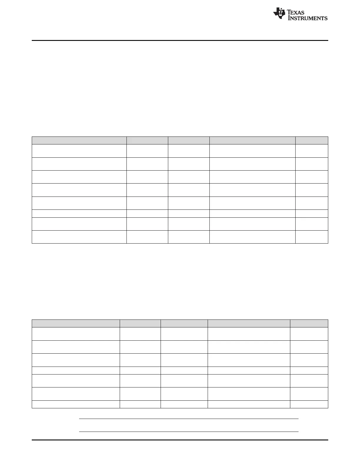
Table 24. Processor’s Secondary/SERDES Ref Clock
Signal/Net Name Probe Point Clock Gen/CH Description Frequency
CLKGEN_SERDES1_REFCLK_P/N R176/ R167 CDCI1/Y1 100MHz HCSL Clock to SoC
SERDES1
100 MHz
CLKGEN_PCIE0_1L_REFCLK_P/N R143/ R142 CDCI1/Y2 100 MHz HCSL Clock to PCIe0 x1 L
Socket
100 MHz
CLKGEN_SERDES0_REFCLK_P/N R145/ R153 CDCI1/Y3 100 MHz HCSL Clock to SoC
SERDES0
100 MHz
CLKGEN_PCIE0_2L_REFCLK_P/N R168/ R177 CDCI1/Y4 100 MHz HCSL Clock to PCIe0 x2 L
Socket
100 MHz
CLKGEN_SERDES2_REFCLK_P/N R158/ R157 CDCI2/Y1 100 MHz HCSL Clock to SoC
SERDES2
100 MHz
CLKGEN_USB_REFCLK_P/N R160/ R159 CDCI2/Y2 100 MHz HCSL Clock to SoC USB 100 MHz
QSGMII_PHY_REFCLK_P/N C108/ C109 CDCI2/Y3 125 MHz LVDS Clock to Ethernet
Expansion board
125 MHz
CLKGEN_PCIE2_2L_REFCLK_P/N R123/ R124 CDCI2/Y4 100 MHz HCSL Clock to PCIe M.2
Socket
100 MHz
The PCIe reference clocks to the PCIe x1, x2 and M.2 sockets are also derived from the CDCI clock
generators.
4.7.3 EVM Peripheral Ref Clock
The reference clocks to the EVM peripherals are sourced by the Clock generator (CDCEL937PWR) on the
Common processor board, which is programmed through I2C0 port of processor. A 24-MHz crystal is
attached to this clock generator to derive the desired clock outputs.
Table 25. EVM Peripheral Ref Clock
Signal/Net Name Probe Point Clock Gen/Ch Description Frequency
USB1_HUB_REFCLK R80 CDCEL/Y1 24 MHz clock for USB Hub (not used
by default)
24 MHz
DSI_REFCLK_1V8 R92 CDCEL/Y2 25 MHz clock for DSI transmitter
('941A)
25 MHz
QSGMII_REFCLK R81 CDCEL/Y3 25 MHz clock for Ethernet Expansion
Board
25 MHz
RGMII_REFCLK R100 CDCEL/Y4 25 MHz clock for Expansion Board 25 MHz
CSI2_REFCLK R101 CDCEL/Y5 25 MHz clock for CSI2 Expansion
Board
25 MHz
OSC0_REFCLK R82 CDCEL/Y6 22.5782 MHz clock for SoC (not
used by default)
22.5782 MHz
EXP_REFCLK R83 CDCEL/Y7 <not currently used> 24 MHz
NOTE: The probe points mentioned above are with reference to Common processor board.

 Loading...


