Do you have a question about the Texas Instruments LMK04828 and is the answer not in the manual?
Specifies the ultra-low RMS jitter performance of the device.
Details the dual loop PLL architecture for improved performance.
Lists wireless infrastructure as a key application area.
Highlights data converter clocking as a primary application.
Provides an overview of the LMK0482x family of clock conditioners.
Compares configuration details across different devices in the family.
Illustrates the pinout of the 64-pin WQFN NKD package.
Details the function of each pin on the device.
Specifies the electrical limits beyond which device damage may occur.
Defines the Electrostatic Discharge protection levels for the device.
Lists the conditions under which the device is guaranteed to operate.
Provides thermal characteristics and resistance values.
Details the current consumption for various device configurations.
Specifies requirements for CLKin and feedback clock inputs.
Details performance parameters for Phase-Locked Loop 1.
Specifies input requirements for the PLL2 reference clock.
Details the performance of the internal Voltage Controlled Oscillators.
Specifies the noise floor characteristics of the clock outputs.
Defines phase noise for closed-loop operation with VCXO.
Specifies jitter performance for closed-loop operation with VCXO.
Specifies default clock output frequencies after reset.
Details parameters related to clock skew and delay.
Specifies electrical characteristics for LVDS clock outputs.
Details electrical characteristics for HSDS clock outputs.
Specifies electrical characteristics for LVPECL clock outputs.
Details electrical characteristics for LVCMOS OSCout.
Specifies characteristics for digital outputs like CLKin_SELX.
Details electrical characteristics for digital inputs.
Phase noise plot for LMK04821 DCLKout2.
Phase noise plot for LMK04826B DCLKout2.
Phase noise plot for LMK04828B DCLKout2.
Defines charge pump current measurement parameters.
Provides a general overview of the LMK0482x family features.
Explains the dual PLL architecture for jitter cleaning.
Details the device's compliance with JEDEC JESD204B standards.
Describes the three redundant reference clock inputs for PLL1.
Explains the frequency holdover operation.
Describes the integrated loop filter components for PLL2.
Details the clock distribution capabilities of the device.
Explains the analog and digital delay features for device clocks.
Describes features for glitchless delay operations.
Details the programmable output types for clock outputs.
Explains the cascaded and nested 0-delay modes.
Describes the function of the device status pins.
Illustrates the functional block diagram for the LMK04821.
Illustrates the functional block diagram for LMK04826 and LMK04828.
Shows the block diagram for device and SYSREF clock outputs.
Illustrates the clocking paths for SYNC and SYSREF signals.
Describes the SYNC and SYSREF functionality.
Details features related to JEDEC JESD204B.
Provides instructions on how to enable SYSREF functionality.
Provides an example setup procedure for SYSREF.
Describes different operating modes for SYSREF.
Details the SYSREF Pulser mode operation.
Explains the fixed digital delay functionality.
Describes the manual mode for input clock switching.
Explains the pin select mode for input clock switching.
Provides method to calculate frequency accuracy for lock detect.
Details how to enable the holdover mode.
Describes manual configuration of CPout1 in holdover mode.
Explains tracked configuration of CPout1 in holdover mode.
Describes device operation while in holdover mode.
Explains the methods for exiting holdover mode.
Details automatic exit criteria for holdover mode.
Describes the typical dual PLL mode of operation.
Outlines the recommended sequence for programming device registers.
Provides a comprehensive map of device registers for programming.
Describes registers related to system functions like RESET.
Details registers containing product identification information.
Provides the IC version identifier register.
Controls clock output levels and device clock dividers.
Controls digital delay high and low count values.
Controls VCO source selection and OSCout parameters.
Sets the division values for SYSREF outputs.
Configures the digital delay values for SYSREF.
Sets the number of SYSREF pulses.
Controls feedback features for PLL2 and PLL1.
Controls power down for OSCin and SYSREF functions.
Enables dynamic digital delay for clocks and SYSREF.
Controls CLKin enable and IO type settings.
Configures CLKin selection mode and output routing.
Configures holdover functions like LOS and DAC tracking.
Sets the holdover digital lock detect count.
Configures the CLKin0 divider for PLL1.
Configures the CLKin1 divider for PLL1.
Configures the CLKin2 divider for PLL1.
Sets the N divider value for PLL1.
Sets the R divider value for PLL2.
Configures PLL2 N divider for calibration.
Disables frequency calibration and sets PLL2 N divider.
Controls PLL2 prescaler and power down settings.
Sets the VCO1 divider value.
Registers for optimizing VCO1 phase noise performance.
Provides readback access to PLL1 lock detect status.
Provides readback access to PLL2 lock detect status.
Provides readback access to CLKin selection and LOS indicators.
Contains the DAC value for user readback.
Provides information on Texas Instruments design tools.
Lists common application scenarios for the device.
Explains how to set frequency accuracy for digital lock detect.
Recommends circuits for driving CLKin pins with differential sources.
Specifies the clock output requirements for the design example.
Outlines the steps for the detailed design procedure.
Discusses the process of selecting the appropriate device.
Provides recommendations for connecting device pins.
Details calculations for current consumption and power dissipation.
Provides general guidelines for PCB layout.
Discusses thermal management considerations for the device.
Information on obtaining device support and documentation.
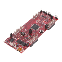
Details available development support tools and resources.
Lists quick access links for technical documents and resources.
Provides a caution regarding electrostatic discharge.
Defines the marketing status of orderable devices.
Provides details on package type, pins, quantity, and finish.
Specifies the dimensions related to tape and reel packaging.
Defines pin 1 orientation for tape and reel assignments.
Provides dimensions for package materials like length, width, height.
Details the dimensions of the WQFN package.
Contains general notes regarding the package outline drawing.
Illustrates an example land pattern for PCB layout.
Provides details on solder mask openings and definitions.
Shows an example stencil design for solderpaste application.
| Brand | Texas Instruments |
|---|---|
| Model | LMK04828 |
| Category | Motherboard |
| Language | English |