LMK04821
,
LMK04826
,
LMK04828
www.ti.com
SNAS605AR –MARCH 2013–REVISED DECEMBER 2015
9.7.3 SYSREF, SYNC, and Device Config
9.7.3.1 VCO_MUX, OSCout_MUX, OSCout_FMT
This register selects the clock distribution source, and OSCout parameters.
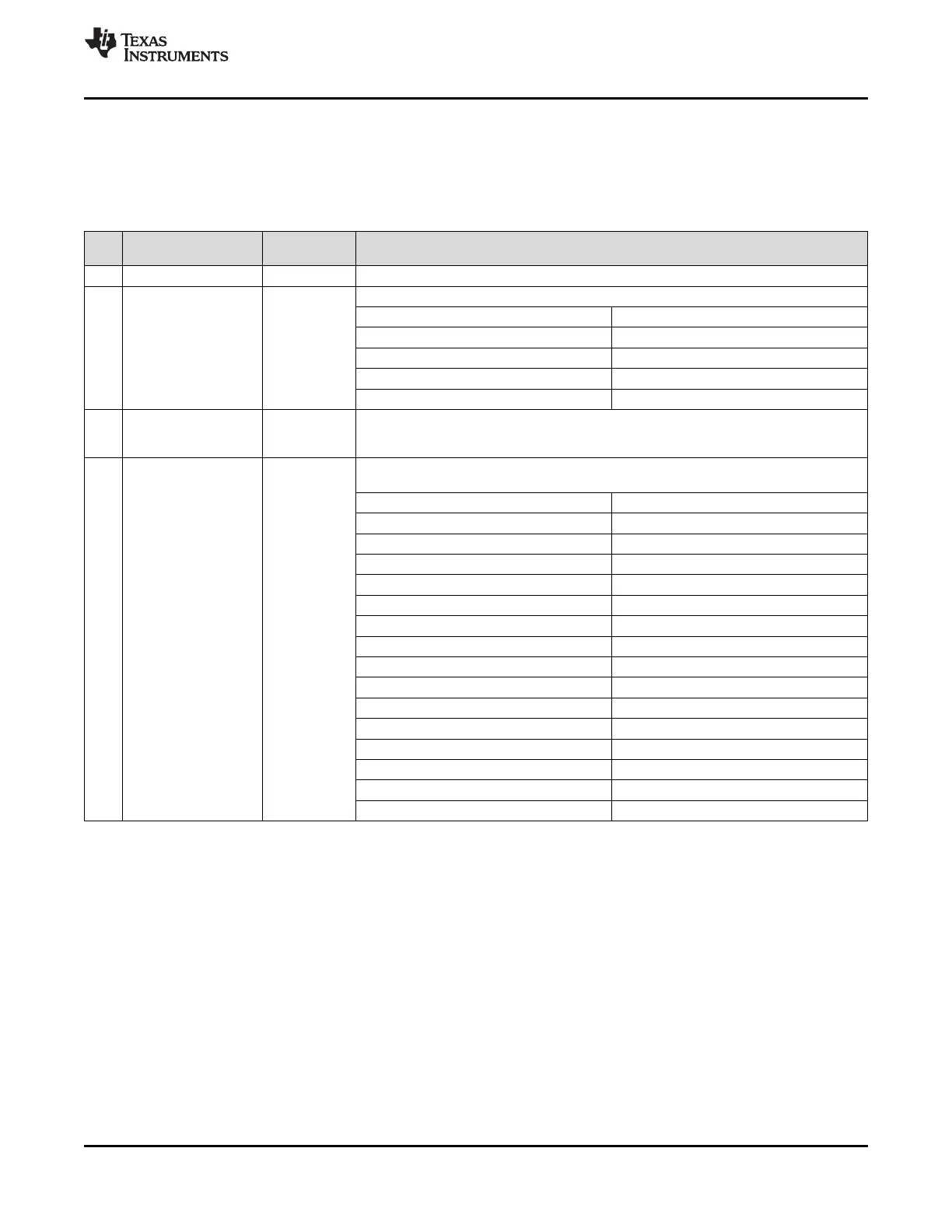
Table 23. Register 0x138
POR
BIT NAME DESCRIPTION
DEFAULT
7 NA 0 Reserved
Selects clock distribution path source from VCO0, VCO1, or CLKin (external VCO)
Field Value VCO Selected
0 (0x00) VCO 0
6:5 VCO_MUX 0
1 (0x01) VCO 1
2 (0x02) CLKin1 (external VCO)
3 (0x03) Reserved
Select the source for OSCout:
4 OSCout_MUX 0 0: Buffered OSCin
1: Feedback Mux
Selects the output format of OSCout. When powered down, these pins may be used as
CLKin2.
Field Value OSCout Format
0 (0x00) Powerdown (CLKin2)
1 (0x01) LVDS
2 (0x02) Reserved
3 (0x03) Reserved
4 (0x04) LVPECL 1600 mVpp
5 (0x05) LVPECL 2000 mVpp
3:0 OSCout_FMT 4
6 (0x06) LVCMOS (Norm / Inv)
7 (0x07) LVCMOS (Inv / Norm)
8 (0x08) LVCMOS (Norm / Norm)
9 (0x09) LVCMOS (Inv / Inv)
10 (0x0A) LVCMOS (Off / Norm)
11 (0x0B) LVCMOS (Off / Inv)
12 (0x0C) LVCMOS (Norm / Off)
13 (0x0D) LVCMOS (Inv / Off)
14 (0x0E) LVCMOS (Off / Off)
Copyright © 2013–2015, Texas Instruments Incorporated Submit Documentation Feedback 61
Product Folder Links: LMK04821 LMK04826 LMK04828