R
CLKinX
CLKinX*
N
Phase
Detector
PLL1
External VCXO
or Tunable
Crystal
R
N
Phase
Detector
PLL2
Dual
Internal
VCOs
External
Loop Filter
OSCin
CPout1
OSCout
OSCout*
LMK0482x
CPout2
Device Clock
Divider
Digital Delay
Analog Delay
SDCLKoutY
SDCLKoutY*
DCLKoutX
DCLKoutX*
Partially
Integrated
Loop Filter
7 Device
Clocks
External
Loop Filter
PLL1 PLL2
7 blocks
Up to 3
inputs
Input
Buffer
SYSREF
Digital Delay
Analog Delay
7 SYSREF
or Device
Clocks
1 Global SYSREF Divider
Up to 1 OSCout
LMK04821
,
LMK04826
,
LMK04828
SNAS605AR –MARCH 2013–REVISED DECEMBER 2015
www.ti.com
9.4 Device Functional Modes
The following section describes the settings to enable various modes of operation for the LMK0482x family. See
Figure 12 and Figure 13 for visual diagrams of each mode.
The LMK0482x Family is a flexible device that can be configured for many different use cases. The following
simplified block diagrams help show the user the different use cases of the device.
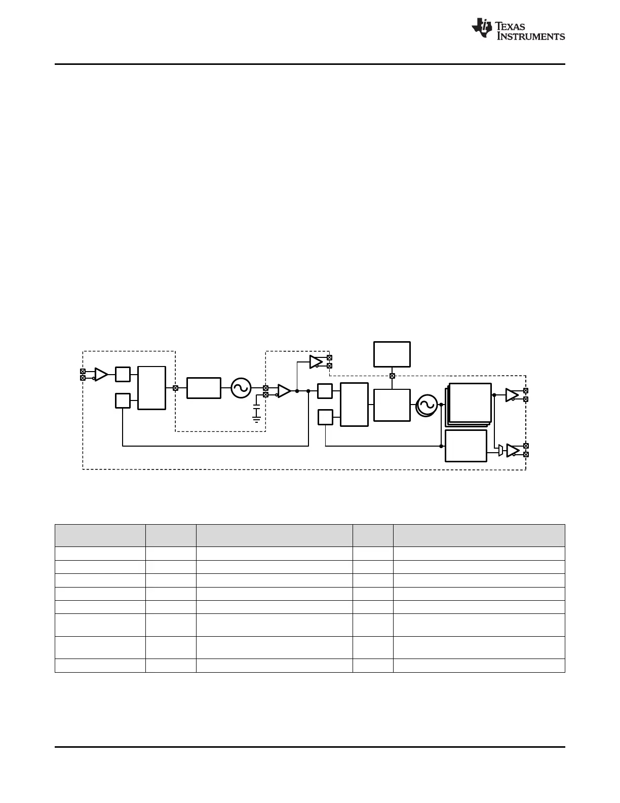
9.4.1 DUAL PLL
Figure 17 illustrates the typical use case of the LMK0482x family in dual loop mode. In dual loop mode the
reference to PLL1 from CLKin0, CLKin1, or CLKin2. An external VCXO or tunable crystal will be used to provide
feedback for the first PLL and a reference to the second PLL. This first PLL cleans the jitter with the VCXO or low
cost tunable crystal by using a narrow loop bandwidth. The VCXO or tunable crystal output may be buffered
through the OSCout port. The VCXO or tunable crystal is used as the reference to PLL2 and may be doubled
using the frequency doubler. The internal VCO drives up to seven divide/delay blocks which drive up to 14 clock
outputs.
Hitless switching and holdover functionality are optionally available when the input reference clock is lost.
Holdover works by fixing the tuning voltage of PLL1 to the VCXO or tunable crystal.
It is also possible to use an external VCO in place of PLL2's internal VCO. In this case one less CLKin is
available as a reference.
LMK04821 includes VCO1 divider on VCO1 output.
Figure 17. Simplified Functional Block Diagram for Dual Loop Mode
Table 5. Dual Loop Mode Register Configuration
REGISTER
FIELD FUNCTION VALUE SELECTED VALUE
ADDRESS
PLL1_NCLK_MUX 0x13F Selects the input to the PLL1 N divider 0 OSCin
PLL2_NCLK_MUX 0x13F Selects the input to the PLL2 N divider 0 PLL2_P
FB_MUX_EN 0x13F Enables the Feedback Mux 0 Disabled
FB_MUX 0x13F Selects the output of the Feedback Mux X Don't care because FB_MUX is disabled
OSCin_PD 0x140 Powers down the OSCin port 0 Powered up
Selects where the output of CLKin0 is
CLKin0_OUT_MUX 0x147 2 PLL1
directed.
Selects where the output of CLKin1 is
CLKin1_OUT_MUX 0x147 2 PLL1
directed.
VCO_MUX 0x138 Selects the VCO 0, 1 or an external VCO 0 or 1 VCO 0 or VCO 1
46 Submit Documentation Feedback Copyright © 2013–2015, Texas Instruments Incorporated
Product Folder Links: LMK04821 LMK04826 LMK04828