LMK04821
,
LMK04826
,
LMK04828
SNAS605AR –MARCH 2013–REVISED DECEMBER 2015
www.ti.com
9.7.8.5 PLL2_WND_SIZE, PLL2_CP_GAIN, PLL2_CP_POL, PLL2_CP_TRI
This register controls the PLL2 phase detector.
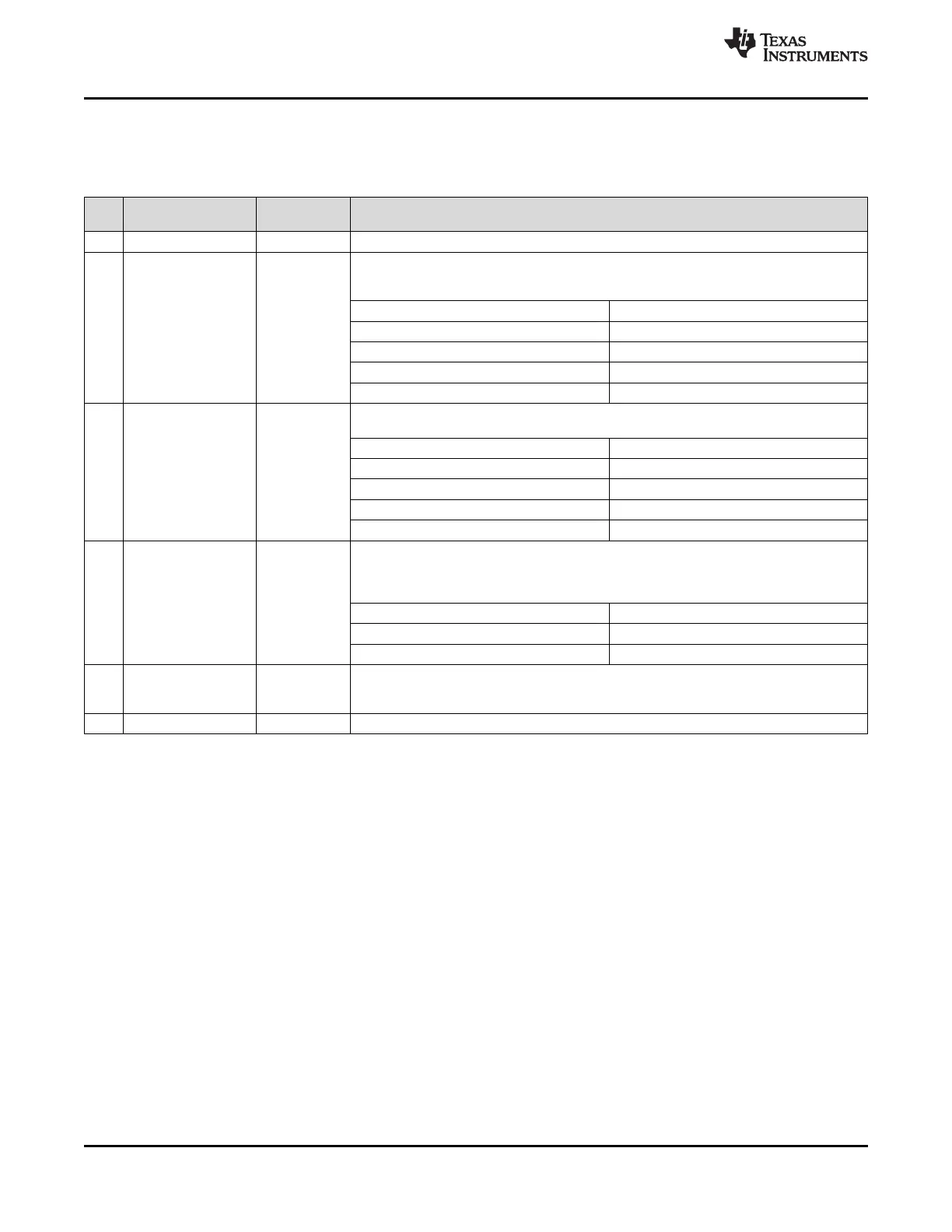
Table 68. Register 0x169
POR
BIT NAME DESCRIPTION
DEFAULT
7 NA 0 Reserved
PLL2_WND_SIZE sets the window size used for digital lock detect for PLL2. If the phase
error between the reference and feedback of PLL2 is less than specified time, then the
PLL2 lock counter increments. This value must be programmed to 2 (3.7 ns).
Field Value Definition
6:5 PLL2_WND_SIZE 2
0 (0x00) Reserved
1 (0x01) Reserved
2 (0x02) 3.7 ns
3 (0x03) Reserved
This bit programs the PLL2 charge pump output current level. The table below also
illustrates the impact of the PLL2 TRISTATE bit in conjunction with PLL2_CP_GAIN.
Field Value Definition
0 (0x00) 100 µA
4:3 PLL2_CP_GAIN 3
1 (0x01) 400 µA
2 (0x02) 1600 µA
3 (0x03) 3200 µA
PLL2_CP_POL sets the charge pump polarity for PLL2. The internal VCO requires the
negative charge pump polarity to be selected. Many VCOs use positive slope.
A positive slope VCO increases output frequency with increasing voltage. A negative slope
VCO decreases output frequency with increasing voltage.
2 PLL2_CP_POL 0
Field Value Description
0 Negative Slope VCO/VCXO
1 Positive Slope VCO/VCXO
PLL2_CP_TRI TRI-STATEs the output of the PLL2 charge pump.
1 PLL2_CP_TRI 0 0: Disabled
1: TRI-STATE
0 Fixed Value 1 When programming register 0x169, this field must be set to 1.
86 Submit Documentation Feedback Copyright © 2013–2015, Texas Instruments Incorporated
Product Folder Links: LMK04821 LMK04826 LMK04828