LMK04821
,
LMK04826
,
LMK04828
SNAS605AR –MARCH 2013–REVISED DECEMBER 2015
www.ti.com
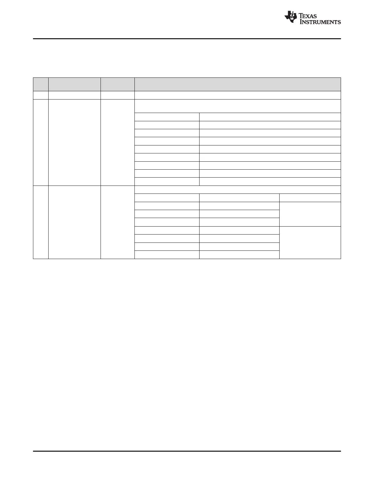
9.7.4.3 CLKin_SEL0_MUX, CLKin_SEL0_TYPE
This register has CLKin_SEL0 controls.
Table 39. Register 0x148
BIT NAME POR
DESCRIPTION
DEFAULT
7:6 NA 0 Reserved
This set the output value of the CLKin_SEL0 pin. This register only applies if
CLKin_SEL0_TYPE is set to an output mode
Field Value Output Format
0 (0x00) Logic Low
1 (0x01) CLKin0 LOS
2 (0x02) CLKin0 Selected
5:3 CLKin_SEL0_MUX 0
3 (0x03) DAC Locked
4 (0x04) DAC Low
5 (0x05) DAC High
6 (0x06) SPI Readback
7 (0x07) Reserved
This sets the IO type of the CLKin_SEL0 pin.
Field Value Configuration Function
0 (0x00) Input Input mode, see Input
Clock Switching - Pin
1 (0x01) Input /w pull-up resistor
Select Mode for
2:0 CLKin_SEL0_TYPE 2 2 (0x02) Input /w pull-down resistor
description of input mode.
3 (0x03) Output (push-pull)
Output modes; the
4 (0x04) Output inverted (push-pull)
CLKin_SEL0_MUX
register for description of
5 (0x05) Reserved
outputs.
6 (0x06) Output (open drain)
70 Submit Documentation Feedback Copyright © 2013–2015, Texas Instruments Incorporated
Product Folder Links: LMK04821 LMK04826 LMK04828