SDIO
(WRITE)
SCLK
CS*
tc
H
tc
S
td
S
t
SCLK
t
HIGH
t
LOW
td
H
SDIO
(Read)
R/W W1
W0
D1 D0
D1 D0
td
V
Data valid only
during read
A12 to A0,
D7 to D2
D7 to
D2
LMK04821
,
LMK04826
,
LMK04828
www.ti.com
SNAS605AR –MARCH 2013–REVISED DECEMBER 2015
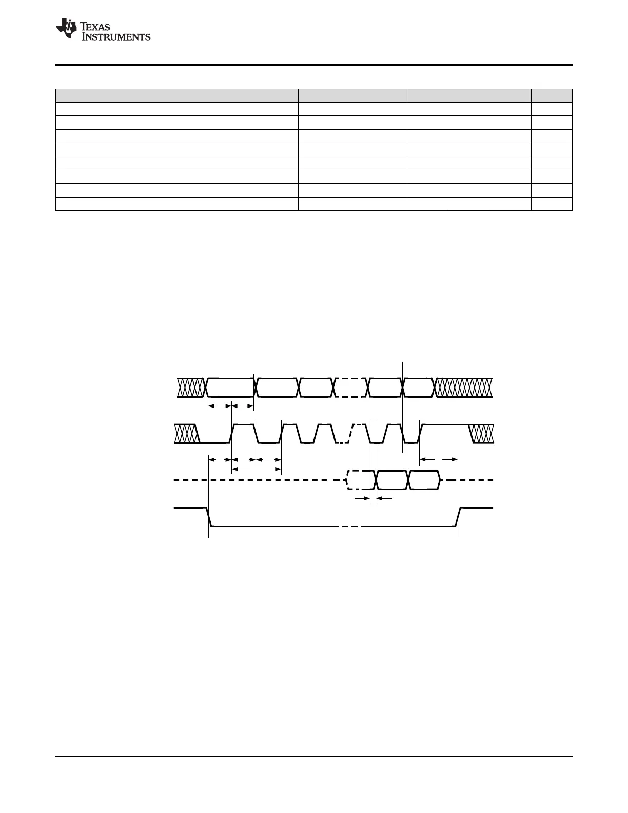
7.6 SPI Interface Timing
TEST CONDITIONS MIN TYP MAX UNIT
td
s
Setup time for SDI edge to SCLK rising edge See Figure 1 10 ns
td
H
Hold time for SDI edge from SCLK rising edge See Figure 1 10 ns
t
SCLK
Period of SCLK See Figure 1 50
(1)
ns
t
HIGH
High width of SCLK See Figure 1 25 ns
t
LOW
Low width of SCLK See Figure 1 25 ns
tc
s
Setup time for CS* falling edge to SCLK rising edge See Figure 1 10 ns
tc
H
Hold time for CS* rising edge from SCLK rising edge See Figure 1 30 ns
td
v
SCLK falling edge to valid read back data See Figure 1 20 ns
(1) 20 MHz
Register programming information on the SDIO pin is clocked into a shift register on each rising edge of the SCK
signal. On the rising edge of the CS* signal, the register is sent from the shift register to the register addressed.
A slew rate of at least 30 V/µs is recommended for these signals. After programming is complete the CS* signal
should be returned to a high state. If the SCK or SDIO lines are toggled while the VCO is in lock, as is
sometimes the case when these lines are shared with other parts, the phase noise may be degraded during this
programming.
4 wire mode read back has same timing as SDIO pin.
R/W bit = 0 is for SPI write. R/W bit = 1 is for SPI read.
W1 and W0 will be written as 0.
Figure 1. SPI Timing Diagram
Copyright © 2013–2015, Texas Instruments Incorporated Submit Documentation Feedback 23
Product Folder Links: LMK04821 LMK04826 LMK04828