0.1 PF
0.1 PF
50:Trace
50:
LMK048XX
Clock Source
CLKinX
CLKinX*
LMK04821
,
LMK04826
,
LMK04828
www.ti.com
SNAS605AR –MARCH 2013–REVISED DECEMBER 2015
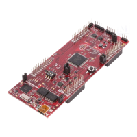
10.2.2.2 Driving CLKin Pins with a Single-ended Source
The CLKin pins of the LMK0482x family can be driven using a single-ended reference clock source, for example,
either a sine wave source or an LVCMOS/LVTTL source. Either AC coupling or DC coupling may be used. In the
case of the sine wave source that is expecting a 50 Ω load, it is recommended that AC coupling be used as
shown in the circuit below with a 50-Ω termination.
NOTE
The signal level must conform to the requirements for the CLKin pins listed in Electrical
Characteristics. CLKinX_BUF_TYPE is recommended to be set to bipolar mode
(CLKinX_BUF_TYPE = 0).
Figure 23. CLKinX/X* Single-ended Termination
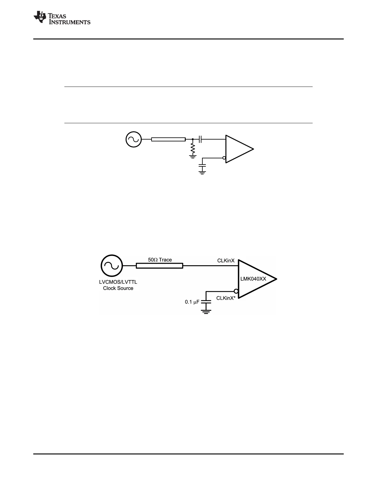
If the CLKin pins are being driven with a single-ended LVCMOS/LVTTL source, either DC coupling or AC
coupling may be used. If DC coupling is used, the CLKinX_BUF_TYPE should be set to MOS buffer mode
(CLKinX_BUF_TYPE = 1) and the voltage swing of the source must meet the specifications for DC coupled,
MOS-mode clock inputs given in Electrical Characteristics. If AC coupling is used, the CLKinX_BUF_TYPE
should be set to the bipolar buffer mode (CLKinX_BUF_TYPE = 0). The voltage swing at the input pins must
meet the specifications for AC coupled, bipolar mode clock inputs given in Electrical Characteristics . In this case,
some attenuation of the clock input level may be required. A simple resistive divider circuit before the AC
coupling capacitor is sufficient.
Figure 24. DC Coupled LVCMOS/LVTTL Reference Clock
Copyright © 2013–2015, Texas Instruments Incorporated Submit Documentation Feedback 97
Product Folder Links: LMK04821 LMK04826 LMK04828