LMK04821
,
LMK04826
,
LMK04828
www.ti.com
SNAS605AR –MARCH 2013–REVISED DECEMBER 2015
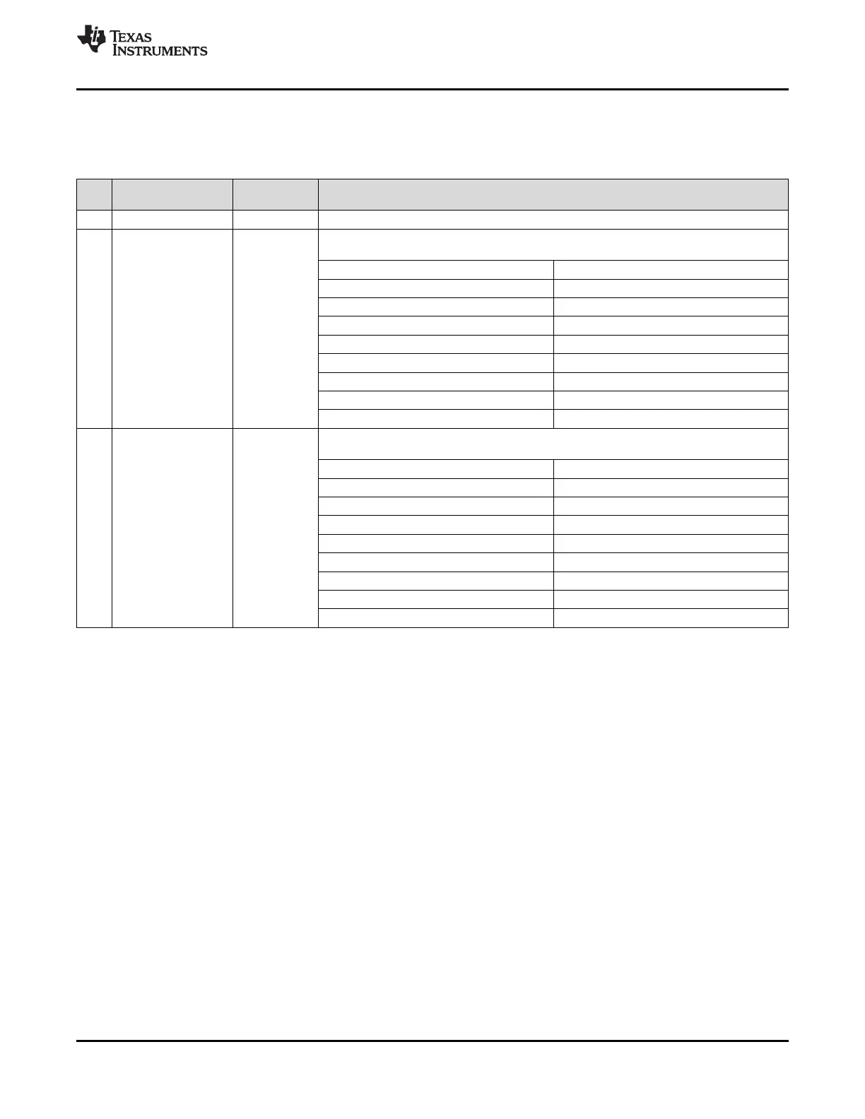
9.7.7.7 PLL1_R_DLY, PLL1_N_DLY
This register contains the delay value for PLL1 N and R delays.
Table 59. Register 0x15E
POR
BIT NAME DESCRIPTION
DEFAULT
7:6 NA 0 Reserved
Increasing delay of PLL1_R_DLY will cause the outputs to lag from CLKinX. For use in 0-
delay mode.
Field Value Gain
0 (0x00) 0 ps
1 (0x01) 205 ps
2 (0x02) 410 ps
5:3 PLL1_R_DLY 0
3 (0x03) 615 ps
4 (0x04) 820 ps
5 (0x05) 1025 ps
6 (0x06) 1230 ps
7 (0x07) 1435 ps
Increasing delay of PLL1_N_DLY will cause the outputs to lead from CLKinX. For use in 0-
delay mode.
Field Value Gain
0 (0x00) 0 ps
1 (0x01) 205 ps
2 (0x02) 410 ps
2:0 PLL1_N_DLY 0
3 (0x03) 615 ps
4 (0x04) 820 ps
5 (0x05) 1025 ps
6 (0x06) 1230 ps
7 (0x07) 1435 ps
Copyright © 2013–2015, Texas Instruments Incorporated Submit Documentation Feedback 81
Product Folder Links: LMK04821 LMK04826 LMK04828