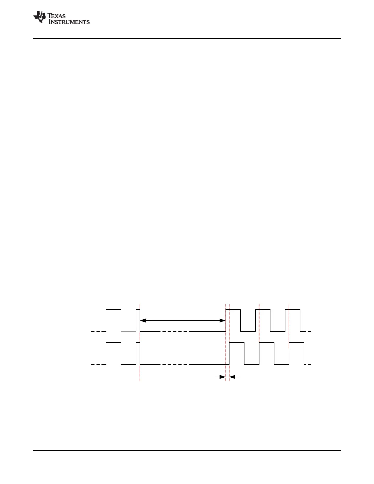
DCLKout0
368.64 MHz
DCLKout2
368.64 MHz
No CLKout during SYNC
SYNC event 1 VCO cycle delay
LMK04821
,
LMK04826
,
LMK04828
www.ti.com
SNAS605AR –MARCH 2013–REVISED DECEMBER 2015
9.3.3 Digital Delay
Digital (coarse) delay allows a group of outputs to be delayed by 4 to 32 VCO cycles. The delay step can be as
small as half the period of the VCO cycle by using the DCLKoutX_HS bit. There are two different ways to use the
digital delay:
1. Fixed digital delay
2. Dynamic digital delay
In both delay modes, the regular clock divider is substituted with an alternative divide value. The substitute divide
value consists of two values, DCLKoutX_DDLY_CNTH and DCLKoutX_DDLY_CNTL. The minimum
_CNTH/_CNTL value is 2 and the maximum _CNTH/_CNTL value is 16. This will result in a minimum alternative
divide value of 4 and a maximum of 32.
9.3.3.1 Fixed Digital Delay
Fixed digital delay value takes effect on the clock outputs after a SYNC event. As such, the outputs will be LOW
for a while during the SYNC event. Applications that cannot accept clock breakup when adjusting digital delay
should use dynamic digital delay.
9.3.3.1.1 Fixed Digital Delay Example
Assuming the device already has the following initial configurations, and the application should delay DCLKout2
by one VCO cycle compared to DCLKout0.
• VCO frequency = 2949.12 MHz
• DCLKout0 = 368.64 MHz (DCLKout0_DIV = 8)
• DCLKout2 = 368.64 MHz (DCLKout2_DIV = 8)
The following steps should be followed
1. Set DCLKout0_DDLY_CNTH = 4 and DCLKout2_DDLY_CNTH = 4. First part of delay for each clock.
2. Set DCLKout0_DDLY_CNTL = 4 and DCLKout2_DDLY_CNTL = 5. Second part of delay for each clock.
3. Set DCLKout0_DDLY_PD = 0 and DCLKout2_DDLY_PD = 0. Power up the digital delay circuit.
4. Set SYNC_DIS0 = 0 and SYNC_DIS2 = 0. Allow the output to be synchronized.
5. Perform SYNC by asserting, then unasserting SYNC. Either by using SYNC_POL bit or the SYNC pin.
6. Now that the SYNC is complete, to save power it is allowable to power down DCLKout0_DDLY_PD = 1
and/or DCLKout2_DDLY_PD = 1.
7. Set SYNC_DIS0 = 1 and SYNC_DIS2 = 1. To prevent the output from being synchronized, very important for
steady state operation when using JESD204B.
Figure 14. Fixed Digital Delay Example
Copyright © 2013–2015, Texas Instruments Incorporated Submit Documentation Feedback 39
Product Folder Links: LMK04821 LMK04826 LMK04828