R
CLKinX
CLKinX*
Phase
Detector
PLL1
External VCXO
or Tunable
Crystal
R
N
Phase
Detector
PLL2
Dual
Internal
VCOs
External
Loop Filter
Input
Buffer
CPout1
OSCout
OSCout*
LMK0482x
CPout2
Divider
Digital Delay
Analog Delay
SDCLKoutY
SDCLKoutY*
DCLKoutX
DCLKoutX*
Partially
Integrated
Loop Filter
7 Device
Clocks
External
Loop Filter
PLL1 PLL2
7 blocks
Up to 3
inputs
N
OSCin
Internal or external loopback, user programmable
SYSREF
Analog Delay
Digital Delay
1 Global SYSREF Divider
7 SYSREF
or Device
Clocks
Up to 1 OSCout
LMK04821
,
LMK04826
,
LMK04828
www.ti.com
SNAS605AR –MARCH 2013–REVISED DECEMBER 2015
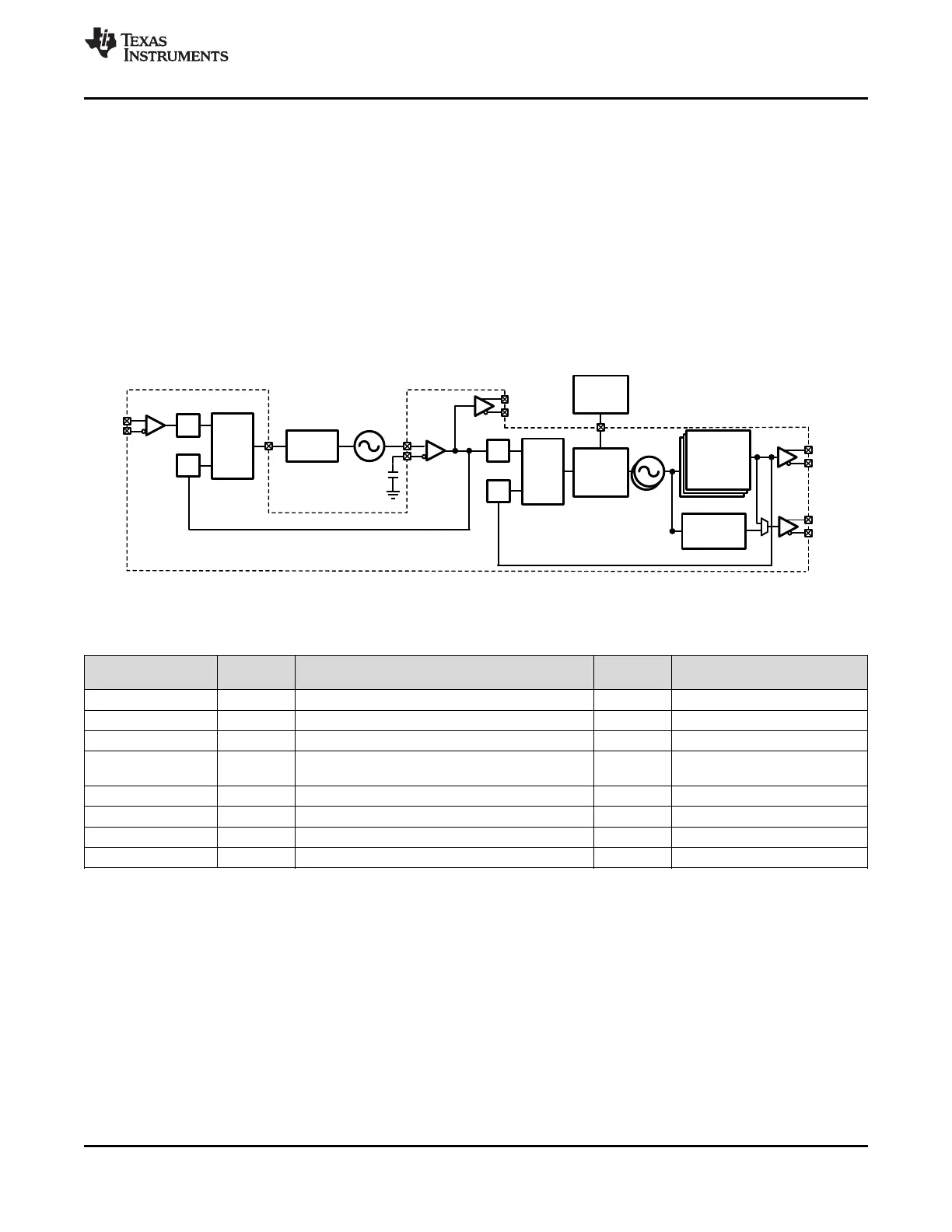
9.4.2 0-DELAY Dual PLL
Figure 18 illustrates the use case of cascaded 0-delay dual loop mode. This configuration differs from dual loop
mode Figure 17 in that the feedback for PLL2 is driven by a clock output instead of the VCO output. Figure 19
illustrates the use case of nested 0-delay dual loop mode. This configuration is similar to the dual PLL in DUAL
PLL except that the feedback to the first PLL is driven by a clock output. This causes the clock outputs to have
deterministic phase relationship with the clock input. Since all the clock outputs can be synchronized together, all
the clock outputs can share the same deterministic phase relationship with the clock input signal. The feedback
to PLL1 can be connected internally as shown using CLKout6, CLKout8, SYSREF, or externally using FBCLKin
(CLKin1).
It is also possible to use an external VCO in place of PLL2's internal VCO; but one less CLKin is available as a
reference and external 0-delay feedback is not available.
LMK04821 includes VCO1 divider on VCO1 output.
Figure 18. Simplified Functional Block Diagram for Cascaded 0-delay Dual Loop Mode
Table 6. Cascaded 0-delay Dual Loop Mode Register Configuration
REGISTER
FIELD FUNCTION VALUE SELECTED VALUE
ADDRESS
PLL1_NCLK_MUX 0x13F Selects the input to the PLL1 N divider. 0 OSCin
PLL2_NCLK_MUX 0x13F Selects the input to the PLL2 N divider 1 Feedback Mux
FB_MUX_EN 0x13F Enables the Feedback Mux. 1 Feedback Mux Enabled
Select between DCLKout6,
FB_MUX 0x13F Selects the output of the Feedback Mux. 0, 1, or 2
DCLKout8, SYSREF
OSCin_PD 0x140 Powers down the OSCin port. 0 Powered up
CLKin0_OUT_MUX 0x147 Selects where the output of CLKin0 is directed. 0 PLL1
CLKin1_OUT_MUX 0x147 Selects where the output of CLKin1 is directed. 0 or 2 Fin or PLL1
VCO_MUX 0x138 Selects the VCO 0, 1 or an external VCO 0 or 1 VCO 0 or VCO 1
Copyright © 2013–2015, Texas Instruments Incorporated Submit Documentation Feedback 47
Product Folder Links: LMK04821 LMK04826 LMK04828