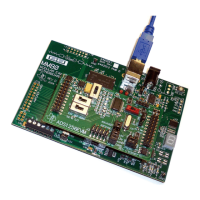
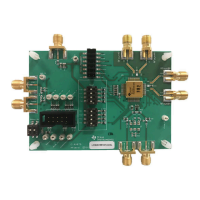
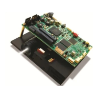
J721E EVM Hardware Architecture
www.ti.com
78
SPRUIS4A–December 2019–Revised May 2020
Submit Documentation Feedback
Copyright © 2019–2020, Texas Instruments Incorporated
Jacinto7 J721E/DRA829/TDA4VM Evaluation Module (EVM)
Table 45. EVM Expansion Connector J51 Pinout (continued)
INFO/GESI Connector Interface J51
Pin No Signal Pin No Signal
95 MCU_ADC1_AIN6 96 NC
97 MCU_ADC1_AIN7 98 NC
99 NC 100 VSYS_IO_3V3
101 NC 102 VSYS_IO_3V3
103 MCU_ADC_EXT_TRIGGER1 104 VSYS_IO_3V3
105 DGND 106 NC
107 I2C6_SCL 108 NC
109 I2C6_SDA 110 NC
111 NC 112 NC
113 USB1_DN4_PE 114 VSYS_IO_1V8
115 USB1_DN4_D_N 116 VSYS_IO_1V8
117 USB1_DN4_D_P 118 VSYS_IO_1V8
119 DGND 120 DGND
4.25 ENET Expansion Connector
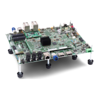
The Common processor board includes an Expansion connector of 171446-1109 with 5 mm mating height
allowing ENET expansion board (Quad-Port Ethernet Expansion) to be stacked on Top side of the
processor board.
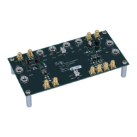
This section provides an overview of the different interfaces and circuits on the Quad port Ethernet
Expansion Board.
4.25.1 Power requirements
The Expansion Card utilizes power from Common processor board through expansion connector and it
has two Low Drop Out circuits to supply Quad Port SGMII PHY with the necessary voltage and the power
required.
Test points for each power outputs are provided on the Ethernet Expansion card and are mentioned in
Table 46.
Table 46. ENET Expansion Board Power Test Points
Sl No Power Supply Test Point Voltage Tolerance
Card Top Side
1 VCC_12V0 C30.1 12 V
2 VSYS_5V0 C34.1 5 V
3 VCC_3V3 C33.1 3.3 V
4 VCC_2V5 TP2 2.5 V
5 VCC_1V TP10 1 V
4.25.2 Clock
4.25.2.1 Main Clock
The Reference clock to the PHY is generated from TI’s Clock Generator Mfr. Part Number#
CDCI6214RGET that is placed on the Common Processor (CPU) Board. Clock inputs shall be AC coupled
and LVDS compliant. The clock generator can be configured by I2C0 of the J721E SoC. The I2C address
of this clock generator is 0x77.
