J721E EVM Hardware Architecture
www.ti.com
64
SPRUIS4A–December 2019–Revised May 2020
Submit Documentation Feedback
Copyright © 2019–2020, Texas Instruments Incorporated
Jacinto7 J721E/DRA829/TDA4VM Evaluation Module (EVM)
The CAN Wake signals of both MCU CAN0 and MAIN CAN0 transceivers are tied together and limited the
voltage level to 1.8V using a Zener diode and terminated to SOM -CP B2B connector.
MAIN CAN2
The MAIN CAN2 port of J721E SoC is connected to the CAN transceiver Mfr. Part# TCAN1042HGVD. A
2-pin header J25 (68002-202HLF) is provided inline for user probe option. This port does not support
WAKE function. The signals MCAN2_H and MCAN2_L are terminated to a 3-pin header J28 (68001-
403HLF) with 120E split termination.
The STB signal is an active High signal held high with external pull up by default. The GPIO control from
MAIN domain provided to pull the line low.
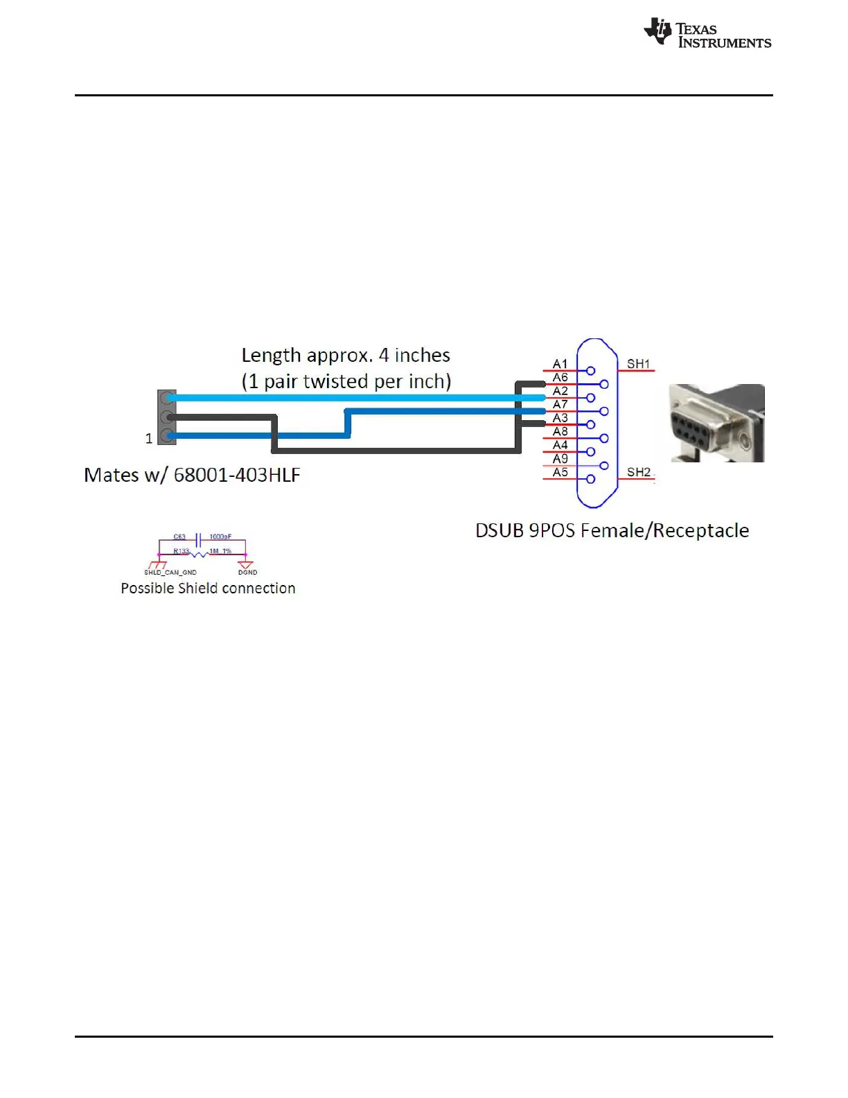
To interface these CAN signals to Test system, the below given custom converter to be prepared.
Figure 48. CAN Header Connections to DB9/Test Instrument