Usage Notes and Known Design Exceptions to Functional Specifications
www.ti.com
32
SPRZ412K–December 2013–Revised February 2020
Submit Documentation Feedback
Copyright © 2013–2020, Texas Instruments Incorporated
TMS320F2837xD Dual-Core MCUs Silicon Revisions C, B, A, 0
Advisory Memory: Prefetching Beyond Valid Memory
Revision(s) Affected 0, A, B, C
Details The C28x CPU prefetches instructions beyond those currently active in its pipeline. If the
prefetch occurs past the end of valid memory, then the CPU may receive an invalid
opcode.
Workaround M1, GS11, GS15 – The prefetch queue is 8 x16 words in depth. Therefore, code should
not come within 8 words of the end of valid memory. Prefetching across the boundary
between two valid memory blocks is all right.
Example 1: M1 ends at address 0x7FF and is not followed by another memory block.
Code in M1 should be stored no farther than address 0x7F7. Addresses 0x7F8–0x7FF
should not be used for code.
Example 2: M0 ends at address 0x3FF and valid memory (M1) follows it. Code in M0
can be stored up to and including address 0x3FF. Code can also cross into M1, up to
and including address 0x7F7.
Flash – The prefetch queue is 16 x16 words in depth. Therefore, code should not come
within 16 words of the end of valid memory; otherwise, it generates a Flash ECC
uncorrectable error.
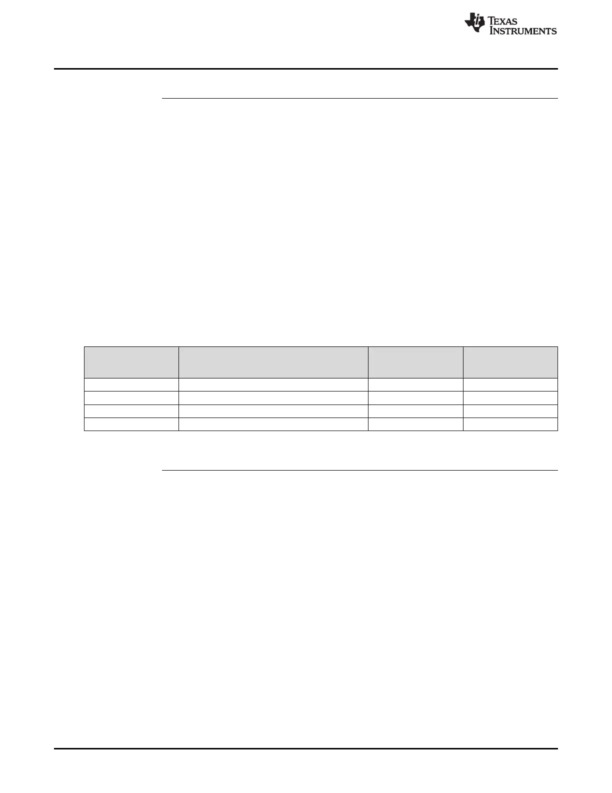
Table 6. Memories Impacted by Advisory
MEMORY TYPE ADDRESSES IMPACTED
F28378D
F28377D
F28375D
F28376D
F28374D
M1 0x0000 07F8–0x0000 07FF Yes Yes
GS11 0x0001 7FF8–0x0001 7FFF No Yes
GS15 0x0001 BFF8–0x0001 BFFF Yes N/A
Flash 0x000B FFF0–0x000B FFFF Yes N/A
Advisory INTOSC: V
DDOSC
Powered Without V
DD
Can Cause INTOSC Frequency Drift
Revision(s) Affected 0, A, B, C
Details The "K" revision of the TMS320F2837xD Dual-Core Microcontrollers Data Manual
(SPRS880K) has updated power sequencing requirements. Revision "J" and earlier
revisions of the data manual did not require V
DDOSC
and V
DD
to be powered on and
powered off at the same time.
If V
DDOSC
is powered on while V
DD
is not powered, there will be an accumulating and
persistent downward frequency drift for INTOSC1 and INTOSC2. The rate of drift
accumulated will be greater when V
DDOSC
is powered without V
DD
at high temperatures.
As a result of this drift, the INTOSC1 and INTOSC2 internal oscillator frequencies could
fall below the minimum values specified in the data manual. This would impact
applications using INTOSC2 as the clock source for the PLL, with the system operating
at a lower frequency than expected.
Workaround(s)
1. Keep V
DDOSC
and V
DD
powered together.
2. Use the external X1 and X2 crystal oscillators as the PLL clock source. The crystal
oscillator does not have any drift related to V
DDOSC
and V
DD
supply sequencing.
 Loading...


