EasyManua.ls Logo

u-blox UBX-G7020 - 4.1 Pin list

u-blox UBX-G7020
74 pages
Print Icon
To Next Page IconTo Next Page
To Previous Page IconTo Previous Page
Loading...
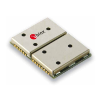
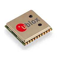
UBX-G7020 - Hardware Integration Manual
Design-in Checklists
GPS.G7-HW-10003 Objective Specification Page 57 of 74
4.1 Pin list
Pin No
MLF40 (WL-
CSP50)
Name
I/O
Description
Remarks
1 (E2)
VDD_ANA
I
Supply for analog part
Has to be supplied by LDO_RF_OUT, pin 38 (F3). It is
recommended to add some filtering, see Figure 5.
2 (E3)
LDO_X_OUT
O
Clock domain voltage
1.0uF to GND. Supply and/ or enable for TCXO
3 (H4)
XTAL_I
I
Main oscillator input
No DC block needed.
4 (H5)
XTAL_O
O
Main oscillator output
Leave open in case TCXO used.
5 (C1)
LDO_B_OUT
O
Backup domain voltage
2.2uF to GND.
6 (C2)
V_BCKP
I
Backup Supply
1.0uF to GND. Connect to VDD_IO if not used.
7 (B1)
VDD_IO
I
PIO and backup supply
1.0uF capacitor to GND.
8 (C3)
USB_DM
I/O
USB data
27 ohm external series resistor. Leave open if not
used.
9 (B2)
VDD_USB
I
USB interface supply
Connect to GND if not used.
10 (B3)
USB_DP
I/O
USB data
27 ohm external series resistor. Leave open if not
used.
11 (A3)
RTC_O
O
RTC oscillator output
Leave open if not used.
12 (A2)
RTC_I
I
RTC oscillator input
Connect to GND if not used.
13 (B4)
PIO14
I
Leave open if not used.
14 (C4)
PIO13
I
Leave open if not used.
15 (A4)
TCK
JTAG interface
Leave open if not used.
16 (C5)
TMS
JTAG interface
Leave open if not used.
17 (B5)
RESET_N
I
Reset input
Leave open if not used.
18 (A6)
PIO7
I
UART RX/ SPI MOSI
UART RX or SPI MOSI, leave open if not used.
19 (A5)
PIO6
O
UART TX/ SPI MISO
UART TX or SPI MISO, leave open if not used.
20 (C6)
T_SENSE
I/O
Temperature sensing
Leave open.
21 (A7)
V_DCDC_IN
I
DCDC converter input
Connect to V_DCDC_O and V_CORE if not used.
22 (B6)
V_DCDC_OUT
O
DCDC converter output
Connect to V_DCDC_I and V_CORE if not used.
23 (C7)
V_CORE
I
Supply for core and RF domain
Connect to main supply or to DCDC converter
inductor.
24 (D7)
LDO_C_OUT
O
Core domain voltage
1.0uF capacitor to GND.
25 (D8)
PIO0
O/I
SQI flash data 0 or config pin
26 (F8)
PIO4
O/I
SQI flash clock or config pin
27 (E8)
PIO2
O/I
SQI flash data 2 or config pin
28 (E7)
PIO1
O/I
SQI flash data 1 or config pin
29 (F7)
PIO5
O/I
SQI flash chip select or CONFIG-
SEL pins
30 (H8)
PIO3
O/I
SQI flash data 3 or config pin
31 (E6)
PIO8
32 (F6)
PIO9
33 (F5)
PIO10
I
D-SEL pin, Selection of Interface
Open=UART and DDC, GND=SPI
34 (H6)
PIO12
I
SAFEBOOT_N pin, to enter Safe
Boot Mode
It is recommended to have a testpoint at
SAFEBOOT_N pin, especially if SQI flash is used
35 (H7)
PIO11
O
TIMEPULSE1, 1PPS
Leave open if not used.
36 (F4)
PIO15
O
Antenna supervisor ANT_OFF
Leave open if not used.
37 (E4)
PIO16
I
Antenna supervisor ANT_OK
Leave open if not used.
38 (F3)
LDO_RF_OUT
O
RF domain voltage
Connect a 1.0uF capacitor to GND. Has to be used to
supply VDD_ANA and VDD_LNA.
39 (H3)
VDD_LNA
I
Supply for LNA
Has to be supplied by LDO_RF_OUT, pin 38 (F3). It is
recommended to add some filtering, see Figure 5.
40 (G1)
LNA_IN
I
RF input
Body (B7, D1, D2,
D3, D4, D5, D6,
E5, F2, H2)
GND
GND
Table 38: pin list
Confidential

Table of Contents

Related product manuals