ZOE-M8 series - Hardware Integration Manual
UBX-16030136 - R07 Production Information Design-in
Page 19 of 32
Add a ground plane underneath the GNSS SiP to reduce interference. This is especially important for the RF
input line.
For improved shielding, add as many vias as possible around the micro strip/coplanar waveguide, around the
serial communication lines, underneath the GNSS SiP, etc.
Calculation of the micro strip for RF input
The micro strip / coplanar waveguide must be 50 Ohms and be routed in a section of the PCB where minimal
interference from noise sources can be expected. Make sure around the RF line is only GND as well as under
the RF line.
In case of a multi-layer PCB, use the thickness of the dielectric between the signal and the 1st GND layer
(typically the 2nd layer) for the micro strip / coplanar waveguide calculation.
If the distance between the micro strip and the adjacent GND area (on the same layer) does not exceed 5 times
the track width of the micro strip, use the “Coplanar Waveguide” model in AppCad to calculate the micro
strip and not the “micro strip” model.
2.12 Layout
This section provides important information for designing a reliable and sensitive GNSS system.
GNSS signals at the surface of the earth are about 15 dB below the thermal noise floor. Signal loss at the antenna
and the RF connection must be minimized as much as possible. When defining a GNSS receiver layout, the
placement of the antenna with respect to the receiver, as well as grounding, shielding and jamming from other
digital devices are crucial issues and need to be considered very carefully.
2.12.1 Footprint
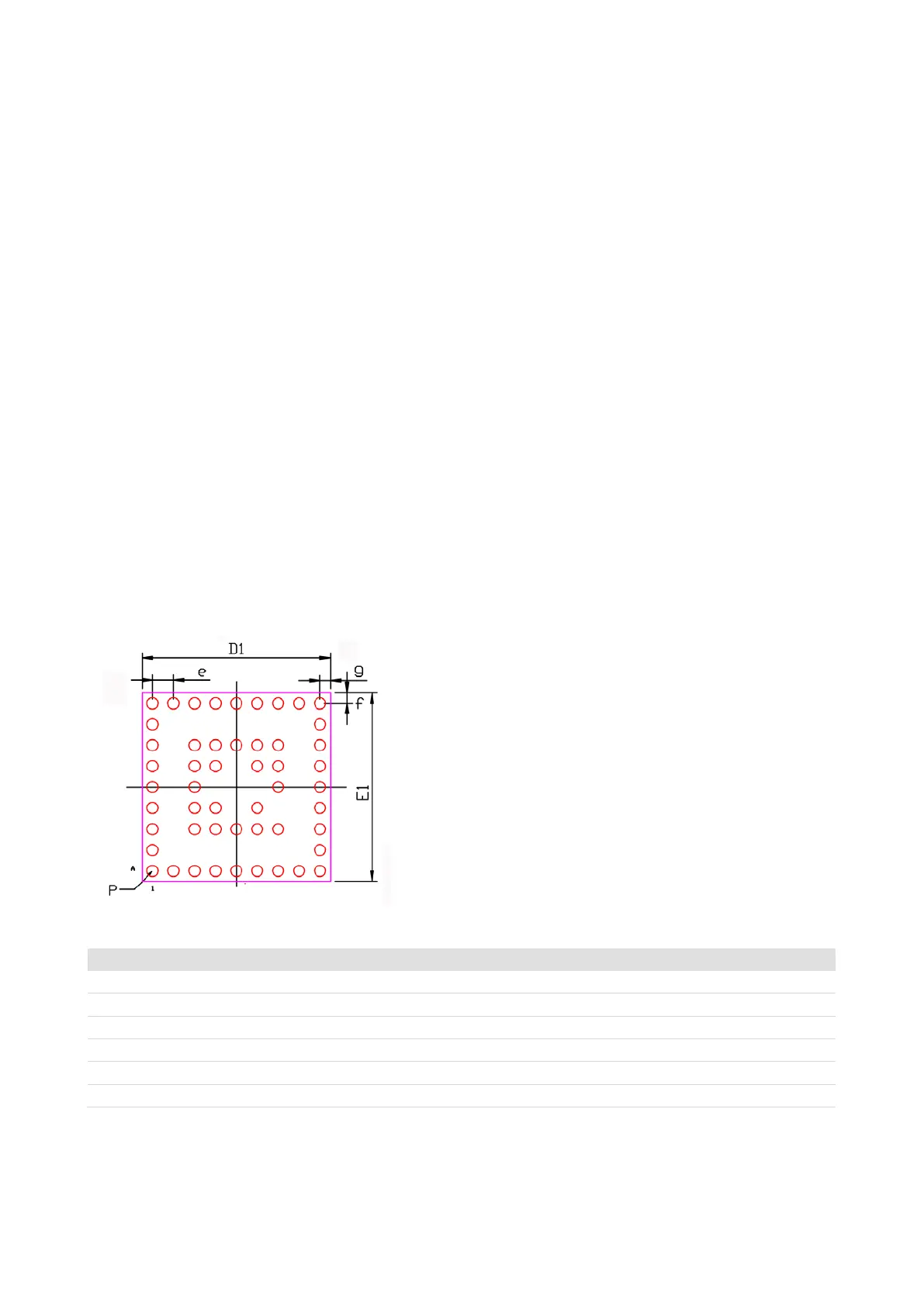
Figure 13: Recommended footprint (bottom view)
Symbol Typ [mm]
e 0.50
g 0.25
f 0.25
D1 4.50
E1 4.50
P 0.27 diameter
Table 4: Footprint dimensions
 Loading...