SARA-R5 series - System integration manual
UBX-19041356 - R04 Design-in Page 51 of 118
C1-Public
☞ ESD sensitivity rating of the VCC supply pins is 1 kV (HBM according to JESD22-A114). Higher
protection level can be required if the line is externally accessible on the application board, e.g. if
accessible battery connector is directly connected to the supply pins. Higher protection level can
be achieved by mounting an ESD protection (e.g. EPCOS CA05P4S14THSG varistor) close to
accessible point.
2.2.1.10 Guidelines for VCC supply layout design
Good connection of the module VCC pins with DC supply source is required for correct RF
performance. Guidelines are summarized in the following list:
• All the available VCC pins must be connected to the DC source.
• VCC connection must be as wide as possible and as short as possible.
• Any series component with Equivalent Series Resistance (ESR) greater than few milliohms must
be avoided.
• VCC connection must be routed through a PCB area separated from RF lines / parts, sensitive
analog signals and sensitive functional units: it is good practice to interpose at least one layer of
PCB ground between the VCC track and other signal routing.
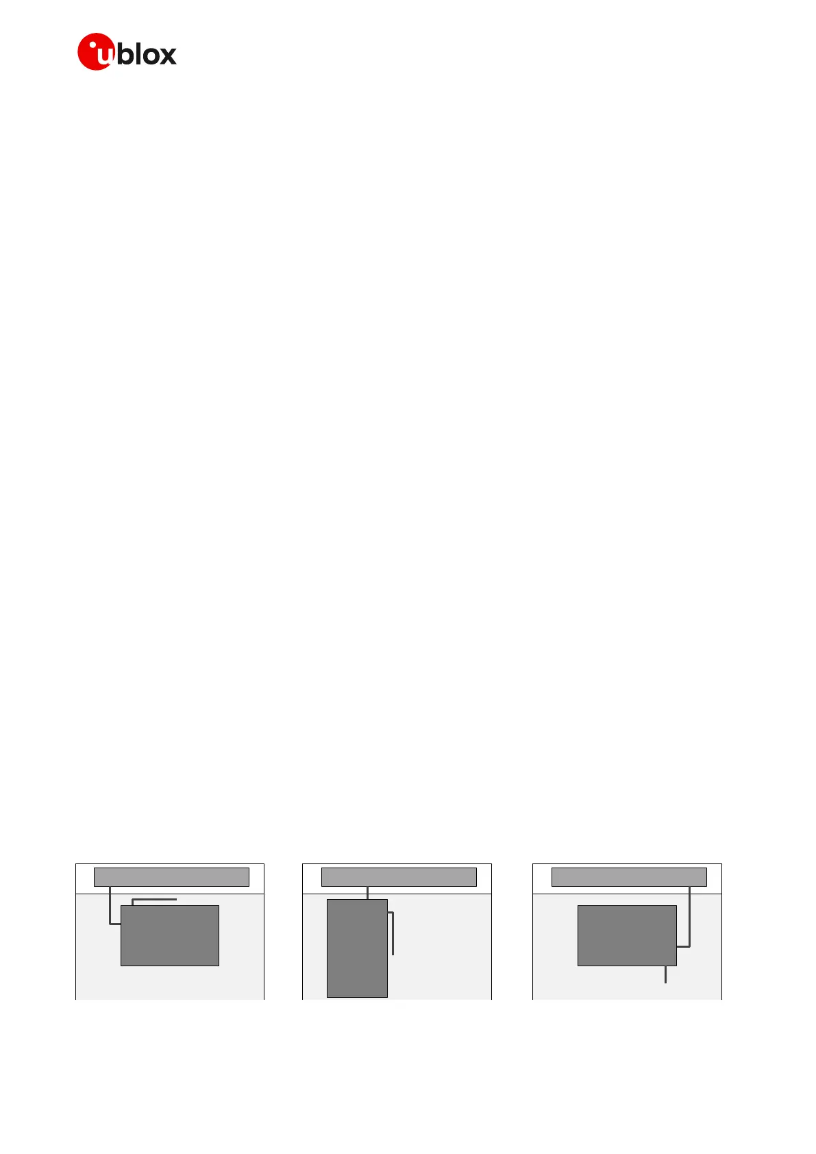
• VCC connection must be routed as far as possible from the antenna, in particular if embedded in
the application device: see Figure 29.
• Coupling between VCC and digital lines must be avoided.
• The tank bypass capacitor for current spikes smoothing described in section 2.2.1.9 should be
placed close to the VCC pins. If the main DC source is a switching DC-DC converter, place the large
capacitor close to the DC-DC output and minimize VCC track length. Otherwise consider using
separate capacitors for DC-DC converter and module.
• The bypass capacitors in the pF range described in Figure 28 and Table 15 should be placed as
close as possible to the VCC pins, where the VCC line narrows close to the module input pins,
improving the RF noise rejection in the band centered on the self-resonant frequency of the pF
capacitors. This is in particular suitable if the application device integrates an internal antenna.
• Since VCC input provides the supply to RF power amplifiers, voltage ripple at high frequency may
result in unwanted spurious modulation of transmitter RF signal. This is more likely to happen with
switching DC-DC converters, in which case it is better to select the highest operating frequency
for the switcher and add a large L-C filter before connecting to the SARA-R5 series modules in the
worst case.
• Shielding of switching DC-DC converter circuit, or at least the use of shielded inductors for the
switching DC-DC converter, may be considered since all switching power supplies may potentially
generate interfering signals as a result of high-frequency high-power switching.
• If VCC is protected by transient voltage suppressor to ensure that the voltage maximum ratings
are not exceeded, place the protecting device along the path from the DC source toward the
module, preferably closer to the DC source (otherwise protection function may be compromised).

 Loading...